Nano-crystalline composite-oxide thin film, environmental gas sensor using the thin film, and method of manufacturing the environmental gas sensor
a composite oxide and thin film technology, applied in the direction of nanostructure manufacture, inorganic chemistry, material resistance, etc., can solve the problems of sensor multi-functionality, sensor has to be robust against wear and time, sensor has to have a high response speed, etc., to achieve excellent gas reactivity characteristics, high selectivity, and high sensitivity
- Summary
- Abstract
- Description
- Claims
- Application Information
AI Technical Summary
Benefits of technology
Problems solved by technology
Method used
Image
Examples
exemplary embodiments 1 to 5
[0060]Nano-Crystalline CuO—Nb-Doped BaTiO3 Composite-Oxide Thin Film for Environmental Gas Sensor
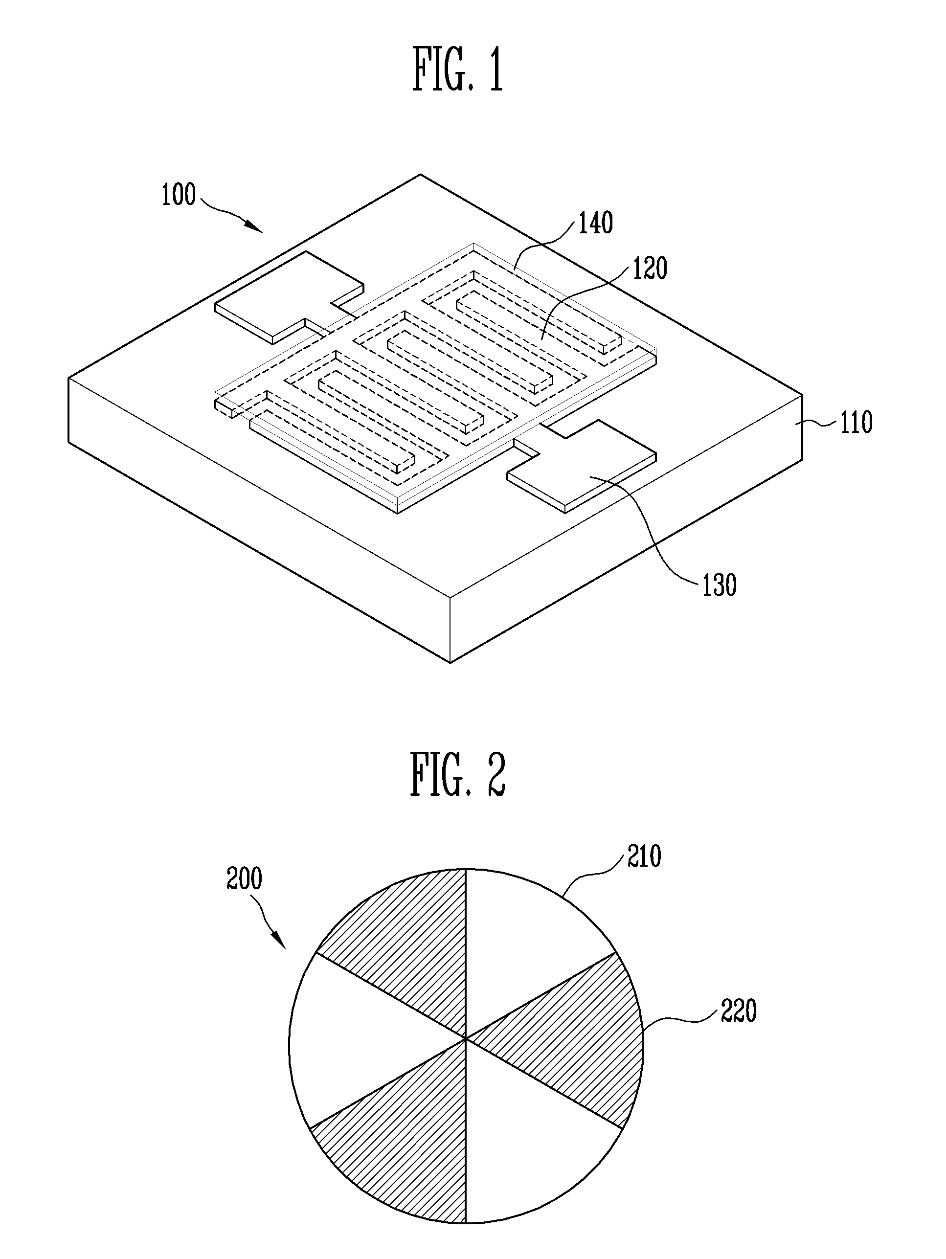
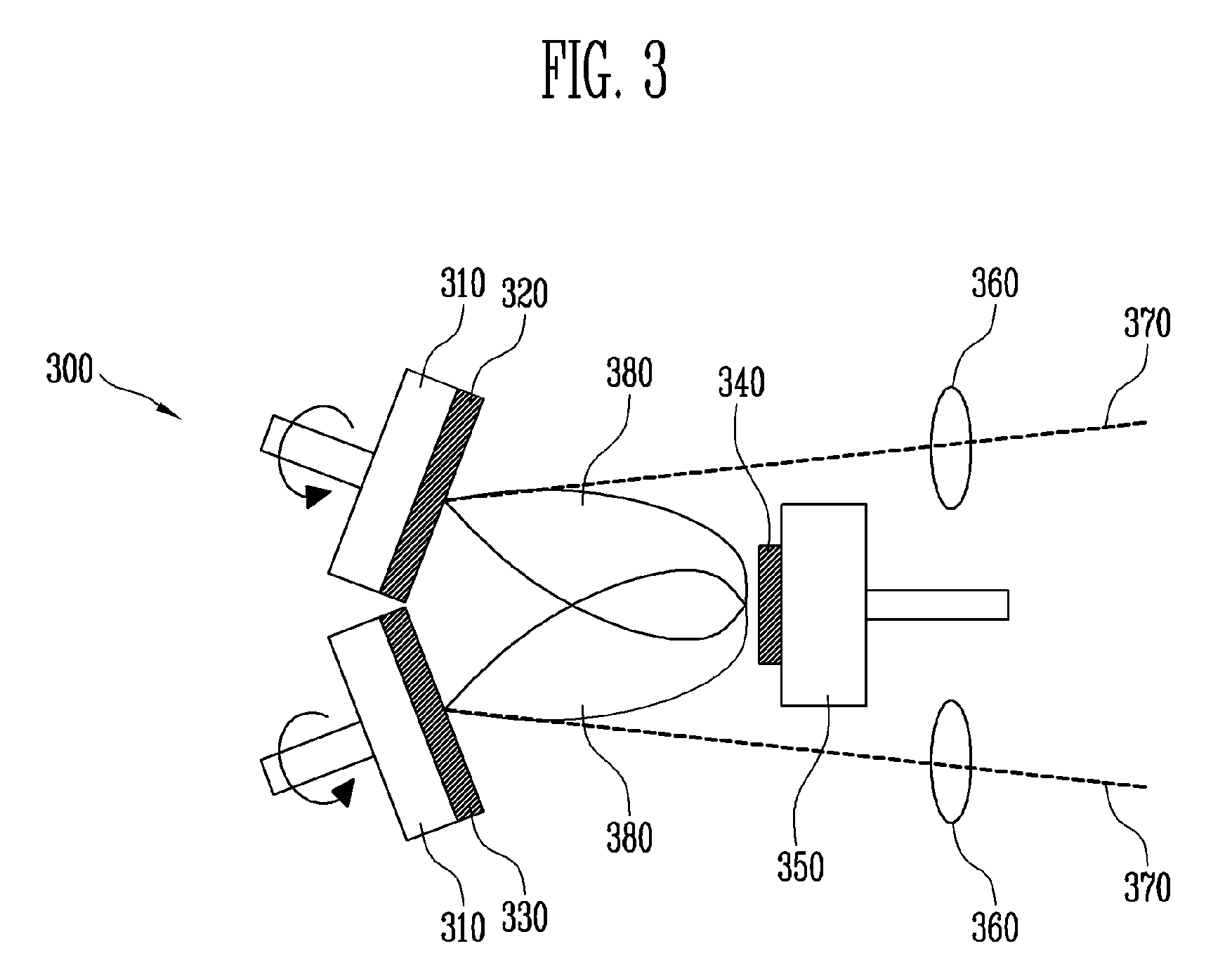
[0061]A CuO oxide ceramic target and an Nb-doped BaTiO3 oxide ceramic target were prepared. A hetero-composite-oxide target was divided into six segments, i.e., three of CuO oxide ceramic A, and three of Nb-doped BaTiO3 oxide ceramic B, which resulted in an ABABAB structure. Subsequently, a nano-crystalline composite-oxide thin film was formed on a MgO (001) single crystalline substrate having a thickness of 0.5 mm by pulse laser ablation using the composite-oxide ceramic target including a composite of the CuO oxide ceramic and the Nb-doped BaTiO3 oxide ceramic. A period of the pulse layer beam and rotational frequency of the composite-oxide target were synchronized such that CuO oxide and Nb-doped BaTiO3 oxide were alternatively deposited on the substrate. Here, the hetero-composite-oxide thin film may be deposited at a temperature ranging from room temperature to 800° C., or deposited...
exemplary embodiments 6 to 11
[0067]Nano-Crystalline CuO—Nb-Doped BaTiO3 Composite-Oxide Thin Film for Environmental Gas Sensor
[0068]A composite-oxide ceramic target having a composite of CuO and Nb-doped BaTiO3 oxide ceramic was prepared by the method of Exemplary embodiment 1, and a nano-crystalline composite-oxide thin film was formed on a SiO2 / Si substrate having a thickness of 0.5 mm by pulse laser ablation. A period of the pulsed laser beam and rotation frequency of the composite-oxide target were synchronized, such that CuO oxide and Nb-doped BaTiO3 oxide were alternatively deposited on the substrate. In the present embodiment, nano-crystalline composite-oxide thin films were formed to a thickness of 144 nm by deposition at various temperatures, e.g., room temperature, 300, 400, 500, 550 and 600° C., and annealing at 600° C.
[0069]Characteristics of the thin films of Exemplary embodiments 6 to 11 were investigated.
[0070]FIG. 7 is a graph of θ-2θ X-ray diffraction patterns of thin films of Exemplary embodim...
exemplary embodiment 12
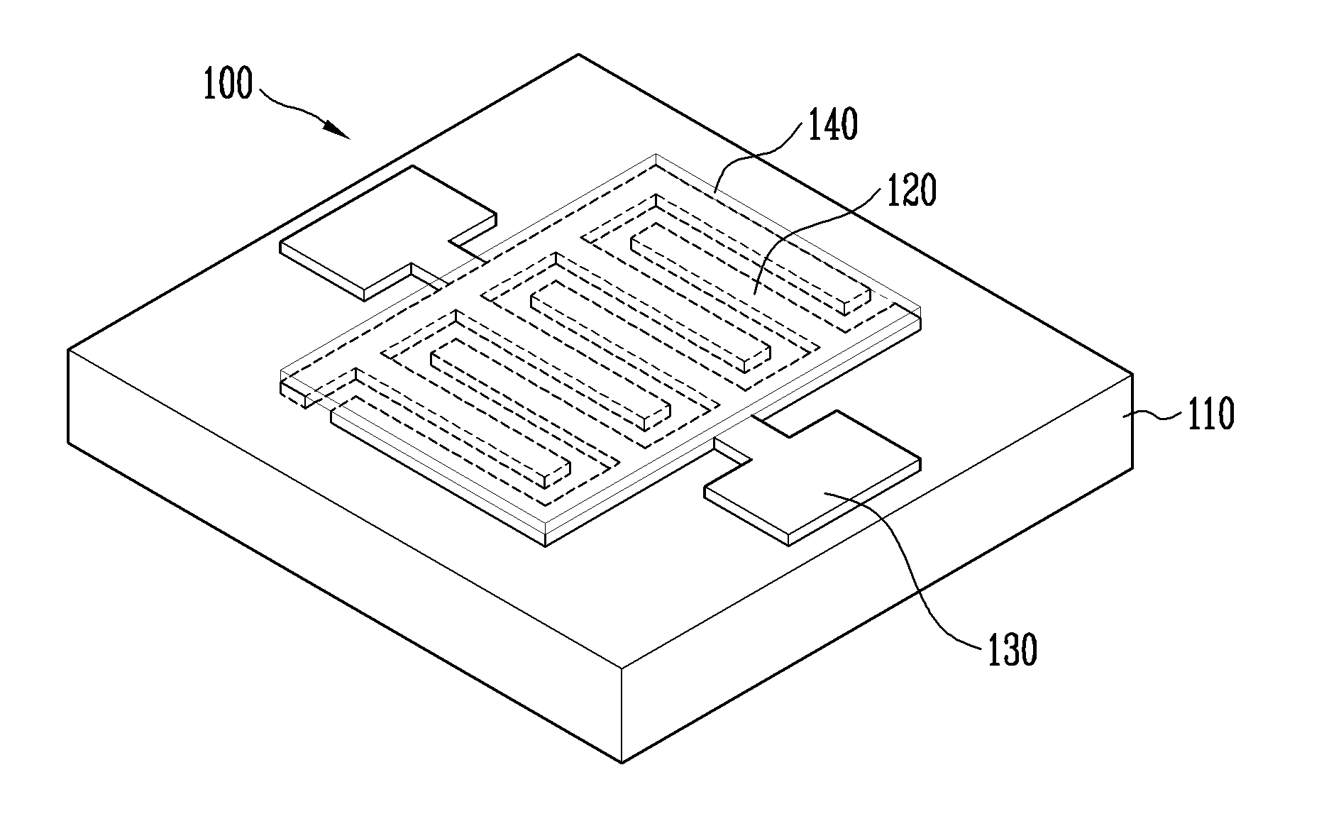
[0072]An interdigitated transducer electrode metal was formed to a thickness of 100 nm on a 0.5 mm SiO2 / Si substrate, and the CuO—Nb-doped BaTiO3 composite-oxide thin film formed in Exemplary embodiment 7 was formed on the electrode metal, such that a capacitive environmental gas sensor having the structure shown in FIG. 1 was manufactured.
[0073]The capacitance and dielectric loss were estimated at different frequencies of the capacitive environmental gas sensor formed in Exemplary embodiment 12. FIG. 9 is a graph of capacitance and dielectric loss versus frequency of the capacitive environmental gas sensor formed in Exemplary embodiment 12. Referring to FIG. 9, the nano-crystalline CuO—Nb-doped BaTiO3 composite-oxide thin film exhibits decreasing capacitance and a dielectric dispersion phenomenon, i.e., anomalous dielectric loss at a grain boundary between hetero nano-crystalline particles around a frequency of 2 kHz.
PUM
| Property | Measurement | Unit |
|---|---|---|
| diameters | aaaaa | aaaaa |
| thickness | aaaaa | aaaaa |
| thickness | aaaaa | aaaaa |
Abstract
Description
Claims
Application Information


