OLED device with substituted acridone compounds

a technology of acridone and acridone, which is applied in the direction of organic semiconductor devices, discharge tubes luminescnet screens, other domestic articles, etc., can solve the problems of low drive voltage, device performance limitations, and many undesirable applications, so as to improve process and display efficiency and improve the effect of efficiency

Active Publication Date: 2009-06-18
GLOBAL OLED TECH
View PDF3 Cites 16 Cited by
  • Summary
  • Abstract
  • Description
  • Claims
  • Application Information

AI Technical Summary

Benefits of technology

[0014]The invention provides an OLED device comprising a cathode, an anode, and having therebetween a layer containing an acridone compound including a diarylamine or carbazole substituent where the nitrogen of the acridone and the nitrogen of the diarylamine or carbazole are connected by an aromatic hydrocarbon linking group. OLED devices of the invention exhibit improved efficiency and drive voltage.

Problems solved by technology

While organic electroluminescent (EL) devices have been known for over two decades, their performance limitations have represented a barrier to many desirable applications.
However, these devices do not have all desired EL characteristics in terms of high efficiency and low drive voltages.

Method used


Image

  • OLED device with substituted acridone compounds
  • OLED device with substituted acridone compounds
  • OLED device with substituted acridone compounds

Examples


experimental examples

Examples 1 and 2

Preparation of Inventive Compounds A-2 and A-1

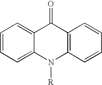
[0312]To an 100 mL dry, three-necked round flask were charged 4-5 bromo-4′-(9-carbazolyl)biphenyl (2.0 g, 5 mmol) (Ref. Chem. Mater. 1998, 10, 2235), 9(10H)-acridone (1.0 g, 5 mmol), K2CO3 (1.0 g, 7.5 mmol), copper (0.33 g, 5 mmol), CuI (0.1 g), 2,2,6,6-tetramethyl-3,5-heptanedione (0.2 g), and MS-dried DMF (30 mL). The mixture was degassed and refluxed under nitrogen atmosphere for 24 h (The reaction may have completed in less than 24 h). After cooling to room temperature, the precipitates from the reaction mixture were collected by filtration, washed with 3 N HCl, water and methanol, and dried in air. The light yellow solid was dissolved in CH2Cl2 (small amount of copper was left as brown particles) and purified by column chromatography on silica gel with CH2Cl2-EtOAc (40:1 v / v) as eluting solvents. The major fraction was collected and evaporation of the solvents afforded 2.1 g of pure product A-2, yield 82%. The materi...

example 3

Preparation of Devices 3.1 through 3.4.

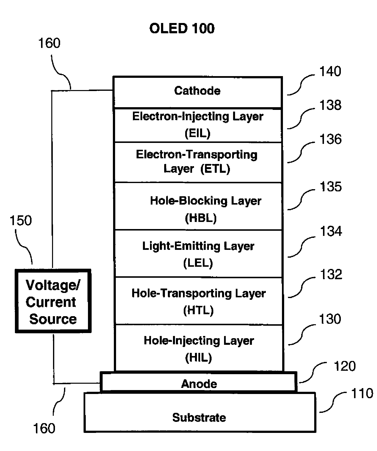
[0313]A series of EL devices (3.1 through 3.4) were constructed in the following manner:[0314]1. A glass substrate coated with an 85 nm layer of indium-tin oxide (ITO), as the anode, was sequentially ultrasonicated in a commercial detergent, rinsed in deionized water, and exposed to oxygen plasma for about 1 min.[0315]2. Over the ITO was deposited a 1 nm fluorocarbon (CFx) hole-injecting layer (HIL) by plasma-assisted deposition of CHF3 as described in U.S. Pat. No. 6,208,075.[0316]3. Next a layer of hole-transporting material 4,4′-Bis[N-(1-naphthyl)-N-phenylamino]biphenyl (NPB) was deposited to a thickness of 75 nm (HTL).[0317]4. Next an exciton block layer (EBL) of 10 nm of 4-(9H-carbazol-9-yl)-N,N-bis[4-(9H-carbazol-9-yl)phenyl]-benzenamine was deposited.[0318]5. A 20 nm light-emitting layer (LEL) composed of host material as listed in Table 1 and 6% phosphorescent dopant Ir(ppy)3 was then deposited.[0319]6. A 50 nm electron-transporting lay...

example 4

Preparation of Devices 4.1 through 4.3.

[0324]A series of EL devices (4.1 through 4.3) were constructed in the same manner as Devices 3.1-3.4 except that the light-emitting phosphorescent material in step 5 was replaced by 1% FD-54, a light-emitting fluorescent material, and the thickness of the ETL in step 6 was decreased to 40 nm.

[0325]The devices thus formed were tested for luminous efficiency at an operating current of 1 mA / cm2 and the results are reported in Table 2.

TABLE 2Experimental ResultsDriveExampleVolt.Efficiency(Type)LEL% EQE(Volts)(cd / A)4.1Comp-12.13.872.58(Comparative)4.2A-14.12.915.67(Inventive4.3A-25.33.435.55(Inventive)

[0326]Table 1 shows experimental results for a LEL using a fluorescent light-emitting compound. The inventive compounds A-1 and A-2, both of which bear one acridone and one diphenylamine or carbazole group, clearly offer improved performance in terms of efficiency and drive voltage relative to Comp-1, which lacks the diarylamino or carbazole group of ...


PUM


Abstract

The invention provides an OLED device comprising a cathode, an anode, and having therebetween a layer containing an acridone compound including a diarylamine or carbazole substituent where the nitrogen of the acridone and the nitrogen of the diarylamine or carbazole are connected by an aromatic hydrocarbon linking group. OLED devices of the invention exhibit improved efficiency and drive voltage.

Description

FIELD OF THE INVENTION[0001]This invention relates to an organic light-emitting diode (OLED) electroluminescent (EL) device that includes acridone compounds substituted with diarylamine or carbazole groups.BACKGROUND OF THE INVENTION[0002]While organic electroluminescent (EL) devices have been known for over two decades, their performance limitations have represented a barrier to many desirable applications. In simplest form, an organic EL device is comprised of an anode for hole injection, a cathode for electron injection, and an organic medium sandwiched between these electrodes to support charge recombination that yields emission of light. These devices are also commonly referred to as organic light-emitting diodes, or OLEDs. Representative of earlier organic EL devices are Gurnee et al. U.S. Pat. No. 3,172,862, issued Mar. 9, 1965; Gurnee U.S. Pat. No. 3,173,050, issued Mar. 9, 1965; Dresner, “Double Injection Electroluminescence in Anthracene”, RCA Review, 30, 322, (1969); and ...

Claims


Application Information

Patent Timeline
Patent Type & Authority Applications(United States)
IPC IPC(8): H01L27/28
CPCH01L51/0061H01L51/0072H01L2251/308H01L51/5016H01L51/5012Y10S428/917H10K85/636H10K85/6572H10K50/11H10K2101/10H10K2102/103
Inventor HUO, SHOUQUANDEATON, JOSEPH C.
Owner GLOBAL OLED TECH
Why Eureka
Try Eureka