Method for manufacturing semiconductor substrate and method for manufacturing semiconductor device

a manufacturing method and semiconductor technology, applied in the direction of manufacturing tools, crystal growth process, after-treatment details, etc., can solve the problems of glass substrate shrinkage when heated, more restrictions on the manufacturing method of soi substrate, and more likely to bend

Inactive Publication Date: 2009-07-02
SEMICON ENERGY LAB CO LTD
View PDF17 Cites 44 Cited by
  • Summary
  • Abstract
  • Description
  • Claims
  • Application Information

AI Technical Summary

Problems solved by technology

However, a glass substrate has disadvantages in that a glass substrate shrinks when heated, has a strain point of 700° C. or lower, is more likely to bend than a silicon wafer, and has an undulating surface, etc.
Due to such disadvantages, there are more restrictions on a method for manufacturing an SOI substrate using a glass substrate as a base substrate than on a method for manufacturing an SOI subs

Method used


Image

  • Method for manufacturing semiconductor substrate and method for manufacturing semiconductor device
  • Method for manufacturing semiconductor substrate and method for manufacturing semiconductor device
  • Method for manufacturing semiconductor substrate and method for manufacturing semiconductor device

Examples


embodiment mode 1

[0082]In this embodiment mode, a semiconductor substrate in which a single crystal semiconductor layer is fixed to a base substrate with a buffer layer interposed therebetween and a manufacturing method thereof are described. In addition, in this embodiment mode, planarization treatment and crystallinity recovery treatment of a single crystal semiconductor layer which is fixed to a base substrate are described.

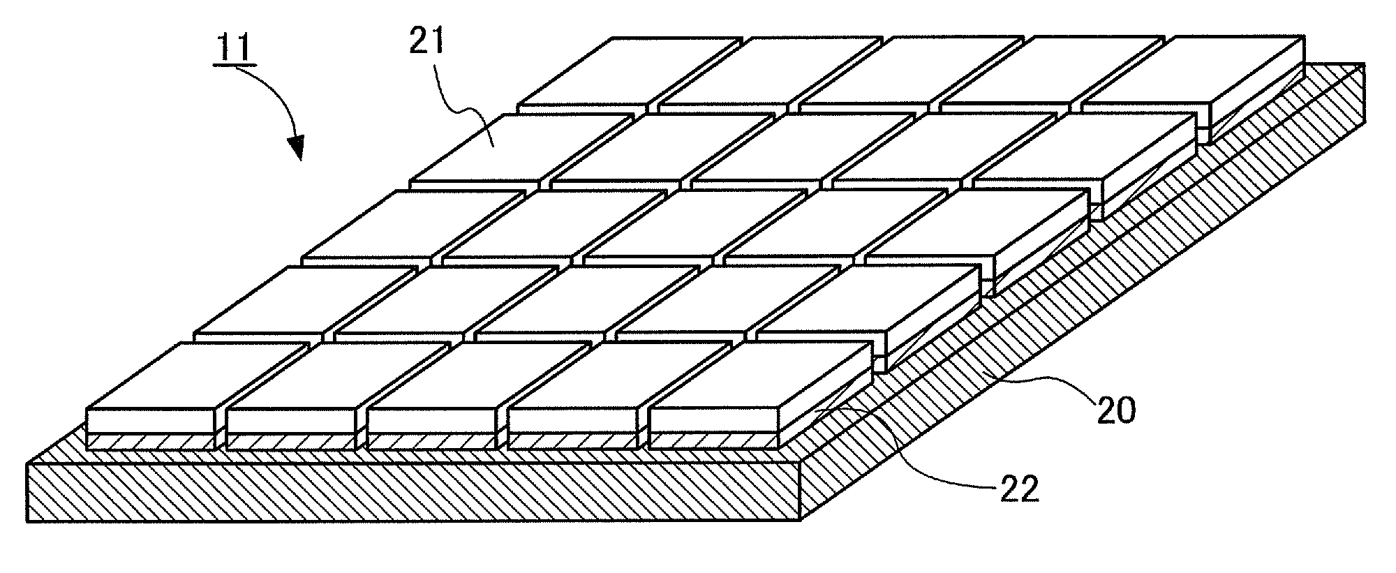
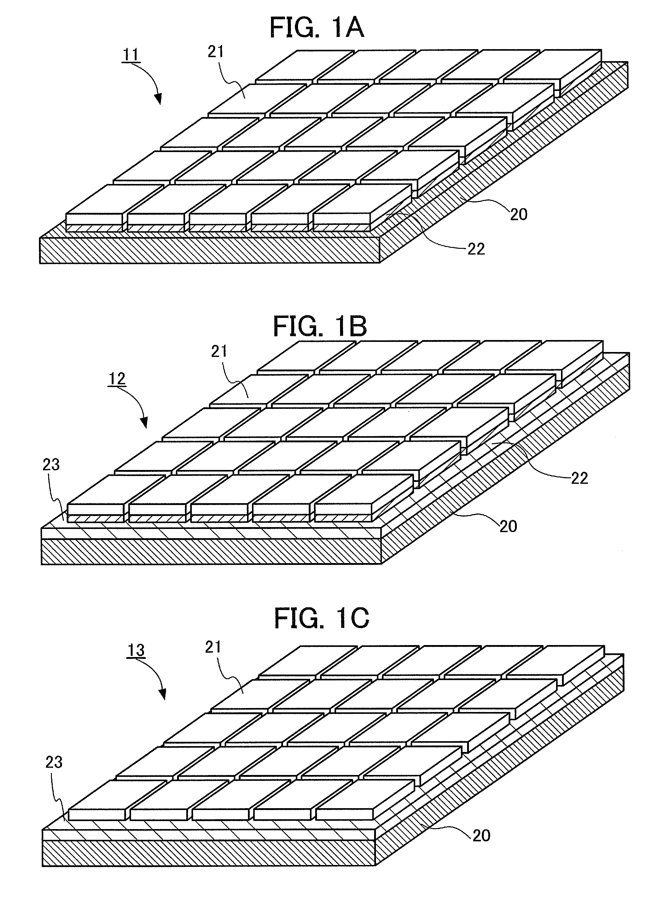
[0083]In this embodiment mode, a structure of a semiconductor substrate is described. FIGS. 1A to 1C are perspective views each illustrating an example of a structure of a semiconductor substrate. Semiconductor substrates 11 to 13 illustrated in FIGS. 1A to 1C are each a substrate in which a plurality of single crystal semiconductor layers 21 is each bonded to one base substrate 20 with an insulating layer interposed therebetween. The single crystal semiconductor layer 21 is a layer formed by division of a single crystal semiconductor substrate. The semiconductor substrates 11...

embodiment mode 2

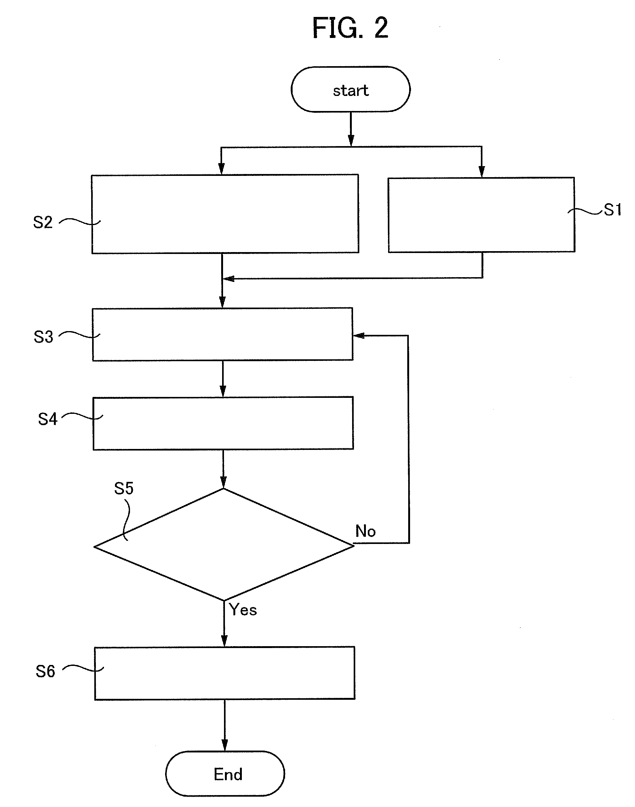
[0099]In this embodiment mode, a method for manufacturing a semiconductor substrate is described. FIG. 2 is a flow chart of a method for manufacturing a semiconductor substrate of the present invention. With the flow of FIG. 2, the semiconductor substrates 11 to 13 illustrated in FIGS. 1A to 1C can be manufactured.

[0100]A base substrate is prepared (Step S1), and a plurality of single crystal semiconductor substrates to be fixed to the base substrate is prepared (Step S2). In Step S1, a buffer layer is formed over a surface of the base substrate as necessary. For example, in the case of manufacturing the semiconductor substrate 12 of FIG. 1B or the semiconductor substrate 13 of FIG. 1C, a base substrate provided with a buffer layer is prepared in Step S1.

[0101]In Step S2, ions (for example, hydrogen ions) are added to a single crystal semiconductor substrate, whereby a damaged region is formed in the single crystal semiconductor substrate at a predetermined depth in order to divide ...

embodiment mode 3

[0196]In this embodiment mode, a method for manufacturing a semiconductor substrate is described. FIG. 12 is a flow chart of the method for manufacturing a semiconductor substrate of this embodiment mode. With the flow of FIG. 12, the semiconductor substrates 11 to 13 illustrated in FIGS. 1A to 1C can be manufactured.

[0197]In FIG. 12, Steps S11 to S15 are similar to Steps S1 to S5 of FIG. 2. A base substrate is prepared (Step S11), and a plurality of single crystal semiconductor substrates to be fixed to the base substrate is prepared (Step S12). In Step S12 of this embodiment mode, hydrogen ions are added to each single crystal semiconductor substrate, whereby a damaged region is formed. Next, substrate fixing treatment is performed (Step S13) to bond the base substrate prepared in Step S11 and one or more of the single crystal semiconductor substrates prepared in Step S12 to each other.

[0198]Next, the one or more of single crystal semiconductor substrates bonded to the base substr...


PUM

PropertyMeasurementUnit
Temperatureaaaaaaaaaa
Melting pointaaaaaaaaaa

Abstract

A semiconductor substrate is manufactured in which a plurality of single crystal semiconductor layers is fixed to a base substrate having low heat resistance such as a glass substrate with a buffer layer interposed therebetween. A plurality of single crystal semiconductor substrates is prepared, each of which includes a buffer layer and a damaged region which is formed by adding hydrogen ions to each semiconductor substrate and contains a large amount of hydrogen. One or more of these single crystal semiconductor substrates is fixed to a base substrate and irradiated with an electromagnetic wave having a frequency of 300 MHz to 300 GHz, thereby being divided along the damaged region. Fixture of single crystal semiconductor substrates and electromagnetic wave irradiation are repeated to manufacture a semiconductor substrate where a required number of single crystal semiconductor substrates are fixed onto the base substrate.

Description

BACKGROUND OF THE INVENTION[0001]1. Field of the Invention[0002]The present invention relates to a method for manufacturing a semiconductor substrate including a single crystal semiconductor layer. The present invention also relates to a method for manufacturing a semiconductor device using a semiconductor substrate including a single crystal semiconductor layer.[0003]2. Description of the Related Art[0004]In recent years, integrated circuits using a silicon-on-insulator (SOI) substrate instead of a bulk silicon wafer have been developed. A feature of a thin single crystal silicon layer formed over an insulating layer can be taken advantage of to form a completely electrically isolated semiconductor layer of a transistor in an integrated circuit and to form a completely depleted transistor. Accordingly, a semiconductor integrated circuit having high added values such as high integration, high-speed operation, and low power consumption can be realized.[0005]A separation-by-implanted-...

Claims


Application Information

Patent Timeline
IPC IPC(8): H01L21/762
CPCB23K26/0075C30B33/04H01L29/66772H01L21/76251H01L21/84H01L21/02686B23K26/3576
Inventor TSUKAMOTO, NAOKISHIMOMURA, AKIHISA
Owner SEMICON ENERGY LAB CO LTD
Why Eureka
Try Eureka