Logic element, and integrated circuit or field programmable gate array

Inactive Publication Date: 2009-07-09
GLOBALFOUNDRIES INC
View PDF2 Cites 5 Cited by
  • Summary
  • Abstract
  • Description
  • Claims
  • Application Information

AI Technical Summary

Benefits of technology

[0027]Logic and memory devices based on the approach according to the invention can be integrated on top of existing (e.g. Si CMOS) circuitry (without consuming Si wafer area) using conventional, low-temperature deposition techniques. Si based elements (such as EEPROM), in contrast, consume Si wafer area or require high-temperature annealing steps (polycrystalline Si) that affect the lower lying layers. Therefore, logic elements based on the invention are Back End of Line (BEOL) compatible. This compatibility allows more dense arrays than EEPROM memory at lower power, lower operating voltage and faster programming speed.
[0028]Also, the logic elements according to the inventi

Problems solved by technology

However, due to gate leakage, static power consumption is increasing with increasing miniaturization.
The need to maintain input voltage will lead to considerable power consumption and heating in future CMOS gene

Method used


Image

  • Logic element, and integrated circuit or field programmable gate array
  • Logic element, and integrated circuit or field programmable gate array
  • Logic element, and integrated circuit or field programmable gate array

Examples


Embodiment Construction

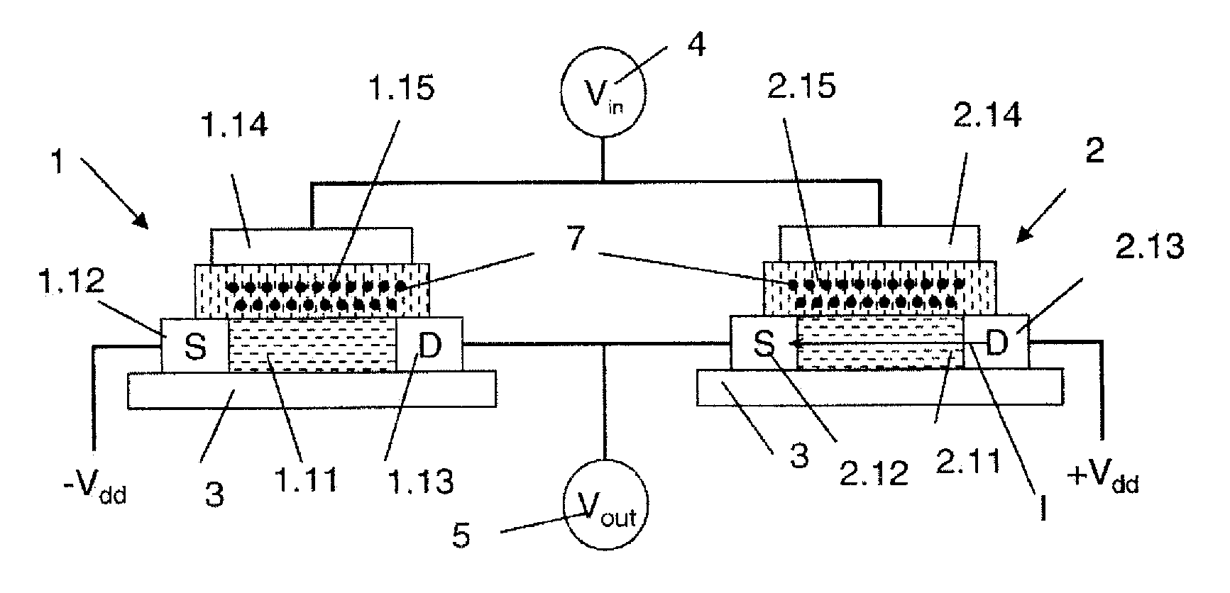
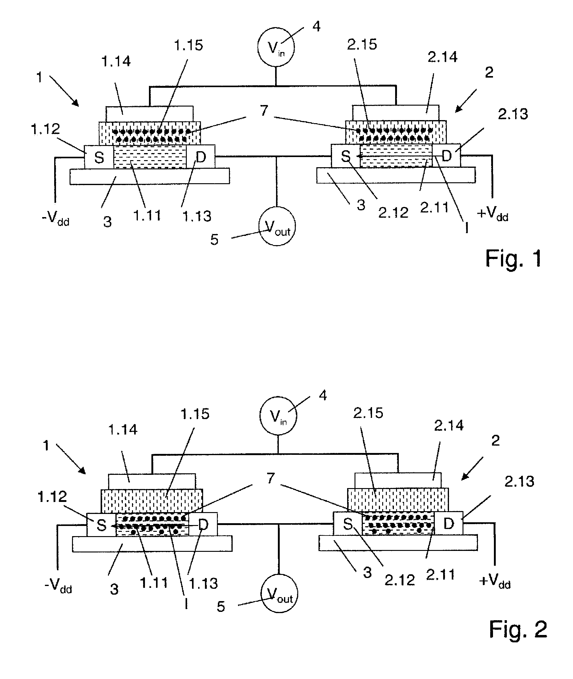
[0038]Referring to FIG. 1, there is shown a logic element that includes a first transistor element 1 and a second transistor element 2. On a substrate 3—that is preferably common to the first and second transistor elements and may be a substrate of a type known for integrated circuits, such as a silicon substrate—the transistor elements 1, 2 comprise a coupling layer 1.11, 2.11 that is in contact with two electrodes S (Source)1.12, 2.12 and D (Drain) 1.13, 2.13. A third electrode 1.14, 2.14, being a gate electrode, is separated from the coupling layer 1.11, 2.11 by an ion conductor layer 1.15, 2.15. The ion conductor layer is an insulating layer having a high oxygen ion mobility. The first coupling layer 1.11 includes a transition metal oxide of a first type, whereas the second coupling layer 2.11 includes a transition metal oxide of a second type.

[0039]Whereas the two transistor elements 1, 2 in this and the following figures are illustrated as separate elements, this need not be t...


PUM


Abstract

A complementary logic element including first and second transistor elements. The first and second gate electrodes of the two transistor elements are electrically parallel to form a common gate. Both the coupling layers of the first and the second transistor element include a resistance switching material, a conductivity of which may be altered by causing an ion concentration to alter if an electrical voltage signal of an appropriate polarity is applied. The first and second transistor elements also include an ion conductor layer that is capable of accepting ions from the coupling layer and of releasing ions into the coupling layer. The coupling layers and ion conductor layers are such that the application of an electrical signal of a given polarity to the gate enhances the electrical conductivity of the first coupling layer and diminishes the electrical conductivity of the second, or vice versa.

Description

CROSS REFERENCE TO RELATED APPLICATION[0001]This application claims priority under 35 U.S.C. 119 from European Patent Application No. 08100278.4 filed Jan. 9, 2008, the entire contents of which are incorporated herein by reference.BACKGROUND OF THE INVENTION[0002]1. Field of the Invention[0003]The present invention relates to a logic element. More particularly, the present invention relates to an integrated circuit or a field programmable gate array that includes such a logic element.[0004]2. Description of Related Art[0005]Complementary logic elements such as CMOS (Complementary metal-oxide-semiconductor) elements are of great importance for integrated circuits. CMOS technology is used in chips such as microprocessors, microcontrollers, static RAM, other digital logic circuits and camera devices. Two important characteristics of CMOS devices are high noise immunity and low static power supply drain. Significant power is only drawn when its transistors are switching between on- and ...

Claims


Application Information

Patent Timeline
IPC IPC(8): H03K19/177H03K19/0944
CPCH01L27/11803H03K19/1778H03K19/17728
Inventor KARG, SIEGFRIED FRIEDRICHMEIJER, GERHARD INGMAR
Owner GLOBALFOUNDRIES INC
Why Eureka
Try Eureka