
Etching composition for an under-bump metallurgy layer and method of forming a bump structure using the same

a technology of etching composition and metallurgy, which is applied in the direction of electrical equipment, semiconductor devices, solid-state devices, etc., can solve the problems of process error, toxic gas such as hydrogen cyanide (hcn) is not generated during a subsequent process, and impurities may remain on the conductive bump, etc., to improve the reliability of eds processes, reduce etching residue or impurities, and reduce the effect of etching

Active Publication Date: 2009-07-09
SAMSUNG ELECTRONICS CO LTD
View PDF11 Cites 21 Cited by
  • Summary
  • Abstract
  • Description
  • Claims
  • Application Information

AI Technical Summary

Benefits of technology

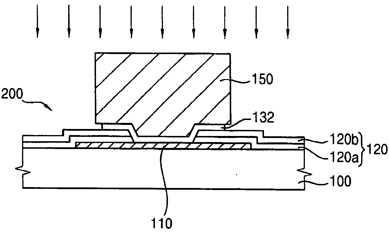
[0009]Exemplary embodiments provide an etching composition for an UBM layer that may reduce and / or prevent impurities that may result during formation of a bump structure from a conductive bump.
[0015]Exemplary embodiments provide an etching composition that may reduce a frequency of a cleaning process for cleaning a probe tip due to impurities, which may be generated during formation of a conductive bump, and may improve productivity.

Problems solved by technology

As a result, a toxic gas such as hydrogen cyanide (HCN) is not generated during a subsequent process.
However, when the conductive bump is formed using a compound without the cyano group, impurities may remain on the conductive bump.
Such impurities may cause a process error during an EDS process.
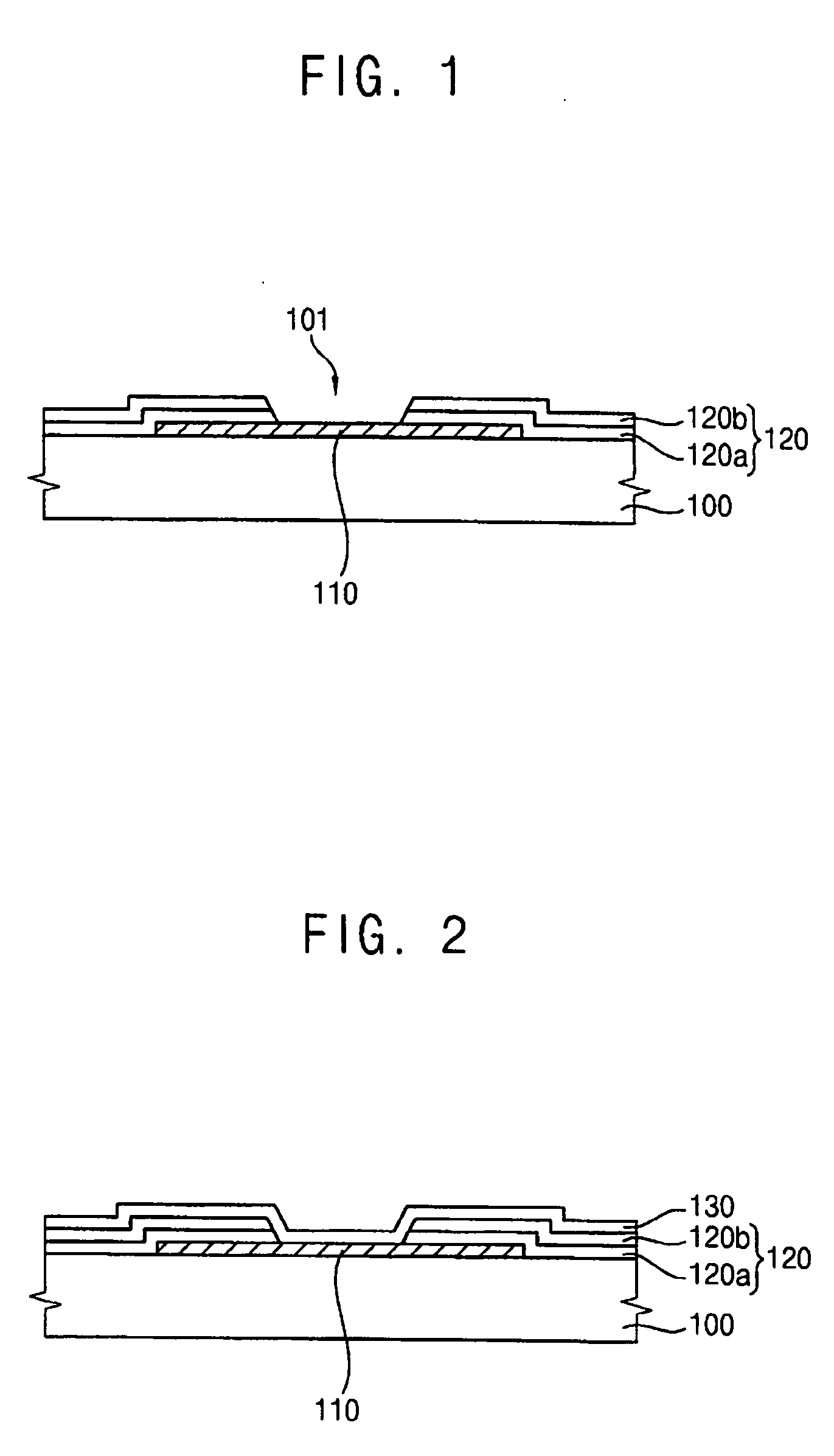
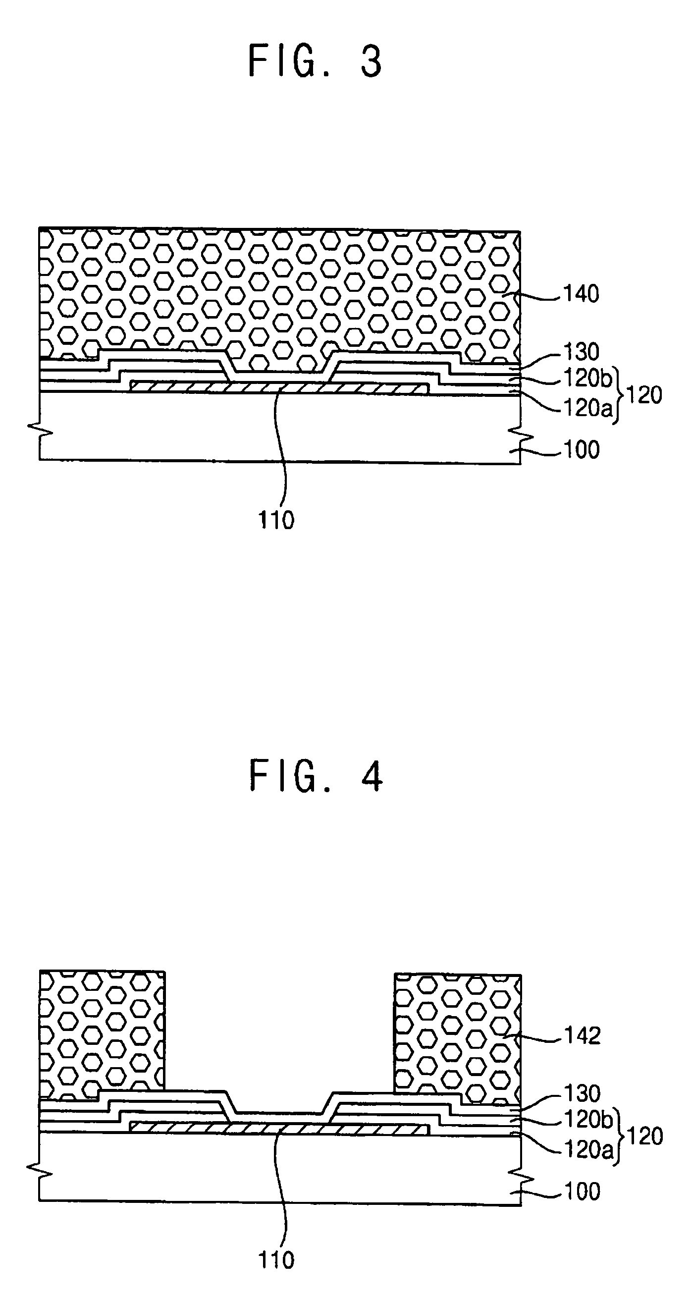
More particularly, when an under-bump metallurgy (UBM) layer exposed by the conductive bump is etched, impurities may be generated and the generated impurities may attach to a probe tip and cause an error in the analysis of an electrical signal.
As a result of such impurities, although a semiconductor chip may be appropriately performed, the probe station may output inappropriate results indicating an electrical short or an electrical open circuit in the semiconductor chip.
However, cleaning processes may be abrasive and may damage the probe tip.
Further, such cleaning processes may not sufficiently remove the impurities from a probe tip.

Method used


Image

  • Etching composition for an under-bump metallurgy layer and method of forming a bump structure using the same
  • Etching composition for an under-bump metallurgy layer and method of forming a bump structure using the same
  • Etching composition for an under-bump metallurgy layer and method of forming a bump structure using the same

Examples


example 1

[0081]A solution including about 79.49% by weight of hydrogen peroxide (H2O2), about 3% by weight of an aqueous basic solution including tetramethylammonium hydroxide (TMAH), about 0.5% by weight of ethyleneglycol (EG), about 17% by weight of ethylenediaminetetraacetic acid dipotassium salt (EDTA-2K) and about 0.01% by weight of a nonionic surfactant NCW (trade name; manufactured by Wako Pure Chemical Industries, Ltd. in Japan) was prepared. The solution was stirred for about 30 minutes to prepare an etching composition for the UBM layer. The aqueous basic solution containing tetramethylammonium hydroxide included about 25% by weight of tetramethylammonium hydroxide.

example 2

[0082]An etching composition was prepared by performing processes substantially the same as that of Example 1 except using about 72.49% by weight of hydrogen peroxide about 10% by weight of an aqueous basic solution including ammonium hydroxide (NH4OH). The aqueous basic solution containing ammonium hydroxide included about 38% by weight of ammonium hydroxide.


PUM

PropertyMeasurementUnit
Temperatureaaaaaaaaaa

Abstract

In an etching composition for an under-bump metallurgy (UBM) layer and a method of forming a bump structure, the etching composition includes about 40% by weight to about 90% by weight of hydrogen peroxide (H2O2), about 1% by weight to about 20% by weight of an aqueous basic solution including ammonium hydroxide (NH4OH) or tetraalkylammonium hydroxide, about 0.01% by weight to about 10% by weight of an alcohol compound, and about 2% by weight to 30% by weight of an ethylenediamine-based chelating agent. The etching composition may effectively etch the UBM layer including titanium or titanium tungsten and remove impurities. A method of forming a bump structure may employ such an etching composition.

Description

BACKGROUND[0001]1. Technical Field[0002]Exemplary embodiments relate to an etching composition for an under-bump metallurgy (UBM) layer, and a method of forming a bump structure. More particularly, exemplary embodiments relate to an etching composition for preventing and / or reducing impurities from being generated on a conductive bump, and a method of forming a bump structure using the same.[0003]2. Description of the Related Art[0004]Generally, a conductive bump is employed for electrically connecting a semiconductor chip with electronic equipment. An electrical die sorting (EDS) process may be performed to examine the performance of the semiconductor chip on which the conductive bump is formed. EDS processes measure electrical characteristics of the semiconductor chip on which the conductive bump is formed using a probe station to confirm whether the semiconductor chip has defects. The probe station includes a probe card for inputting / outputting an electrical signal through a prob...

Claims


Application Information

Patent Timeline
IPC IPC(8): H01L21/441
CPCC23F1/38H01L2924/01033H01L24/11H01L2224/13099H01L2224/16H01L2924/01011H01L2924/01013H01L2924/01018H01L2924/01022H01L2924/01029H01L2924/01046H01L2924/01047H01L2924/01074H01L2924/01078H01L2924/01079H01L2924/14H01L2924/01005H01L2924/01006H01L2924/01019H01L2924/01023H01L2924/01024H01L21/32134H01L2224/05027H01L2224/05022H01L2224/05001H01L2224/05572H01L2224/05124H01L2224/05147H01L2224/05644H01L2224/05655H01L2224/05664H01L2224/05666H01L2224/05671H01L2224/05684H01L24/03H01L24/05H01L2924/00014
Inventor KANG, DONG-MINKANG, BO-RAMKIM, YOUNG-NAMLIM, YOUNG-SAM
Owner SAMSUNG ELECTRONICS CO LTD
Learn More