Method for forming a gate insulating film

Inactive Publication Date: 2009-07-16
RPX CORP
View PDF6 Cites 10 Cited by
  • Summary
  • Abstract
  • Description
  • Claims
  • Application Information

AI Technical Summary

Benefits of technology

[0039]The method for forming a gate insulating film of the present invention can implement an excellent film quality with small oxygen deficiency and l

Problems solved by technology

In the conventional ALD method, however, the exposure time to a material gas and the exposure time to an oxidizing agent during deposition are determined by the productivity and the ALD deposition theory, and are not determined by the capa

Method used


Image

  • Method for forming a gate insulating film
  • Method for forming a gate insulating film
  • Method for forming a gate insulating film

Examples


first example embodiment

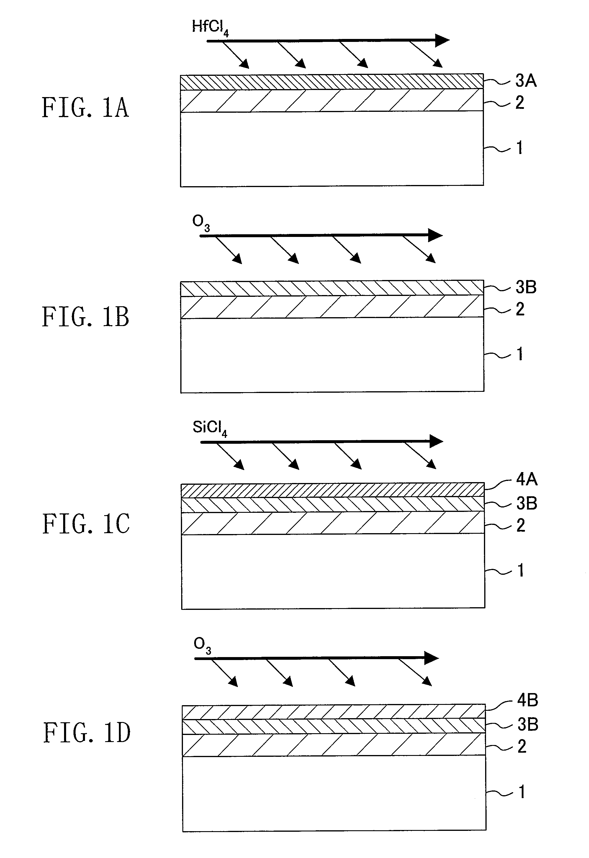
[0054]A first example embodiment will now be described with reference to the figures.

[0055]FIGS. 1A through 1D show cross-sectional structures sequentially illustrating the steps of a method for forming a gate insulating film according to the first example embodiment.

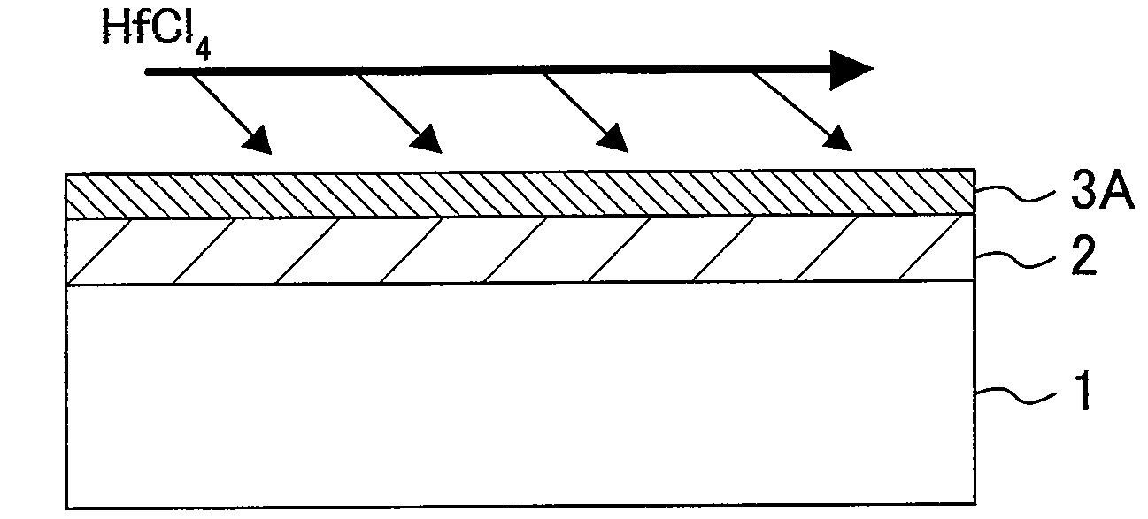
[0056]First, as shown in FIG. 1A, an interface layer 2 is formed on a main surface of a semiconductor substrate 1 before a high dielectric constant metal silicate film is formed. More specifically, the interface layer 2 is formed on an active region where a gate insulating film is to be formed. The semiconductor substrate 1 is made of silicon and the interface layer 2 is made of silicon oxide (SiO2). The interface layer 2 is formed between the gate insulating film made of a high dielectric constant metal silicate and the semiconductor substrate 1. The interface between the semiconductor substrate 1 and the high dielectric constant metal silicate film is thus made of silicon oxide (SiO2), whereby interface characteristic...

second example embodiment

[0080]Hereinafter, a second example embodiment will be described with reference to the figures.

[0081]FIGS. 7A through 7D show cross-sectional structures sequentially illustrating the steps of a method for forming a gate insulating film according to the second example embodiment.

[0082]First, as shown in FIG. 7A, an interface layer 2 is formed on a main surface of a semiconductor substrate 1 in the same manner as that of the first example embodiment. The interface layer 2 is formed on an active region where a gate insulating film is to be formed. The semiconductor substrate 1 is made of silicon and the interface layer 2 is made of SiO2. The surface of the interface layer 2 is then nitride, and the interface layer 2 is thus made of silicon oxynitride (SiON). An annealing process is then performed in an oxygen atmosphere.

[0083]The semiconductor substrate 1 is then held in, for example, a single-wafer chamber having a shower head in a gas introducing portion. Tetrakis-di-methyl-amino-haf...


PUM

PropertyMeasurementUnit
Temperatureaaaaaaaaaa
Fractionaaaaaaaaaa

Abstract

In formation of a gate insulating film made of a high dielectric constant metal silicate, atomic layer deposition (ALD) is performed by setting exposure time to a precursor containing a metal or the like to saturation time of a deposition rate by a surface adsorption reaction and by setting exposure time to an oxidizing agent to time required for a composition of a metal oxide film to reach 97% or more of a stoichiometric value.

Description

CROSS-REFERENCE TO RELATED APPLICATIONS[0001]This application claims priority under 35 U.S.C. §119(a) on Japanese Patent Application No. 2008-3336 filed on Jan. 10, 2008, the entire contents of which are hereby incorporated by reference.BACKGROUND OF THE INVENTION[0002]1. Field of the Invention[0003]The present invention generally relates to a method for forming a gate insulating film. More particularly, the present invention relates to a method for forming a gate insulating film made of a high dielectric constant metal silicate or a high dielectric constant metal oxide.[0004]2. Related Art[0005]With recent improvement in integration degree, functions, and operation speed of semiconductor integrated circuit devices, dimensions of semiconductor elements such as transistors have been reduced. Therefore, not only lateral dimensions of semiconductor elements (dimensions in an in-plane direction of a substrate) such as the gate length of transistors but also longitudinal dimensions there...

Claims


Application Information

Patent Timeline
IPC IPC(8): H01L21/469
CPCC23C16/40H01L29/517H01L21/02148H01L21/02156H01L21/02161H01L21/02164H01L21/02181H01L21/02192H01L21/02238H01L21/02255H01L21/0228H01L21/02332H01L21/02337H01L21/0234H01L21/28194H01L21/28202H01L21/3141H01L21/31608H01L21/31645H01L29/513C23C16/45531
Inventor YONEDA, KENJIYAMAMOTO, KAZUHIKO
Owner RPX CORP
Why Eureka
Try Eureka