Transparent conductive film deposition apparatus, film deposition apparatus for continuous formation of multilayered transparent conductive film, and method of forming the film

a technology of transparent conductive film and deposition apparatus, which is applied in the direction of chemical vapor deposition coating, coating, semiconductor devices, etc., can solve the problems of reducing the performance of solar cells, reducing the efficiency of solar cells, and reducing the need for maintenance, so as to improve the efficiency of utilization of raw materials and reduce the need for maintenance. , the effect of high thermal conductivity

Inactive Publication Date: 2009-08-13
SHOWA SHELL SEKIYU KK
View PDF10 Cites 8 Cited by
  • Summary
  • Abstract
  • Description
  • Claims
  • Application Information

AI Technical Summary

Benefits of technology

[0022]In the invention, each deposition treatment part in the multilayer deposition treatment part is equipped inside with a group of nozzles of a planar structure comprising pipe-form nozzles which have ejection holes formed on the ejection side thereof for simultaneously or separately spraying the three raw materials consisting of the organometallic compound, diborane, and pure water and are arranged adjacently to each other in the same plane without leaving a space between these, and is further equipped with a nozzle-cooling mechanism which cools the group of nozzles. Because of this constitution, the group of nozzles have a one-plate structure having no space between the nozzles. As a result, a reaction product can be prevented from accumulating on the nozzles and the efficiency of utilization of raw materials can be improved. Furthermore, the prevention of reaction product accumulation on the nozzles can further reduce the necessity of maintenance.
[0023]In the invention, the setter may be made of a member having high thermal conductivity (carbon composite) whose surface is coated with a metallic coating having high thermal conductivity and high mechanical strength (e.g., nickel deposit) This constitution enables an even transparent conductive film to be formed. Furthermore, by disposing pins for substrate fixing on the setter, a substrate having any desired size can be treated.
[0018](5) The invention provides the film deposition apparatus for the continuous formation of a multilayered transparent conductive film as described under (1), (2), or (3) above, wherein the nozzle-cooling mechanism comprises either a group of cooling pipes arranged adjacently to each other or a platy cooler, wherein the group of cooling pipes or the platy cooler is disposed on the group of nozzles of a planar structure on the side (back side) opposite to the ejection side.

Problems solved by technology

In the case of the sputtering method, however, the transparent conductive film is known to cause damage to the buffer layer, rather than enhances its effect, and to reduce the performances of the solar cell.
This MOCVD-method film deposition apparatus is not one for continuously forming a transparent conductive film having a multilayer structure, and has had a problem that it cannot form a transparent conductive film having a large area.
However, this apparatus for continuous film deposition is not one for forming a transparent conductive film by the MOCVD method but one for forming a thin semiconductor film.
There has been a problem that it is difficult to directly divert such an apparatus for continuously forming a thin semiconductor film to the continuous formation of a transparent conductive film by the MOCVD method.
There has been a problem that nozzle maintenance is necessary because the temperature of the nozzles rises during growth due to the heat emitted from the hot plate and a deposit accumulates on the nozzles.
Furthermore, there has been a problem that since the related-art nozzle structure has spaces between the ejection parts for an organometallic compound, water, and diborane, product accumulation occurs on the back side of the nozzles and even on an upper part of the chamber, resulting in a low efficiency of utilization of the raw materials and the necessity of frequent maintenance.
There has hence been a problem that in case where the hot plate has an uneven heat distribution, a transparent conductive film which is uneven in sheet resistance, etc. is formed.
There has hence been a problem that the rate of substrate treatment is low and the rate of film deposition is low.

Method used


Image

  • Transparent conductive film deposition apparatus, film deposition apparatus for continuous formation of multilayered transparent conductive film, and method of forming the film
  • Transparent conductive film deposition apparatus, film deposition apparatus for continuous formation of multilayered transparent conductive film, and method of forming the film
  • Transparent conductive film deposition apparatus, film deposition apparatus for continuous formation of multilayered transparent conductive film, and method of forming the film

Examples


Embodiment Construction

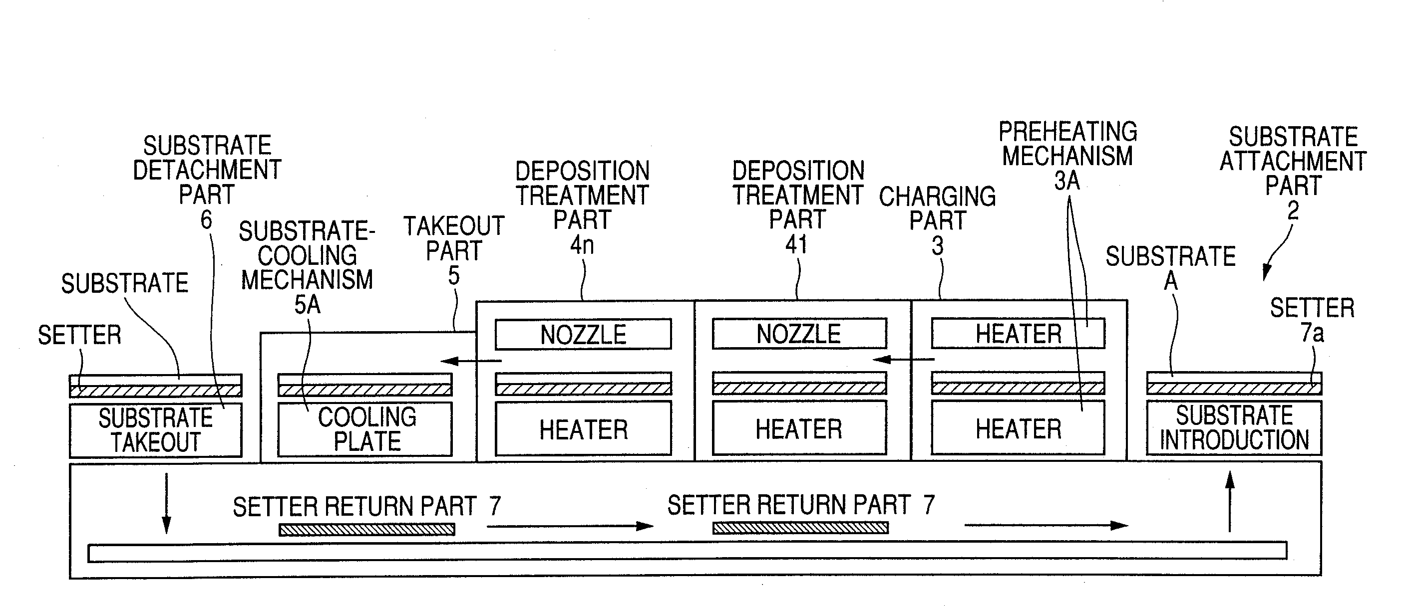
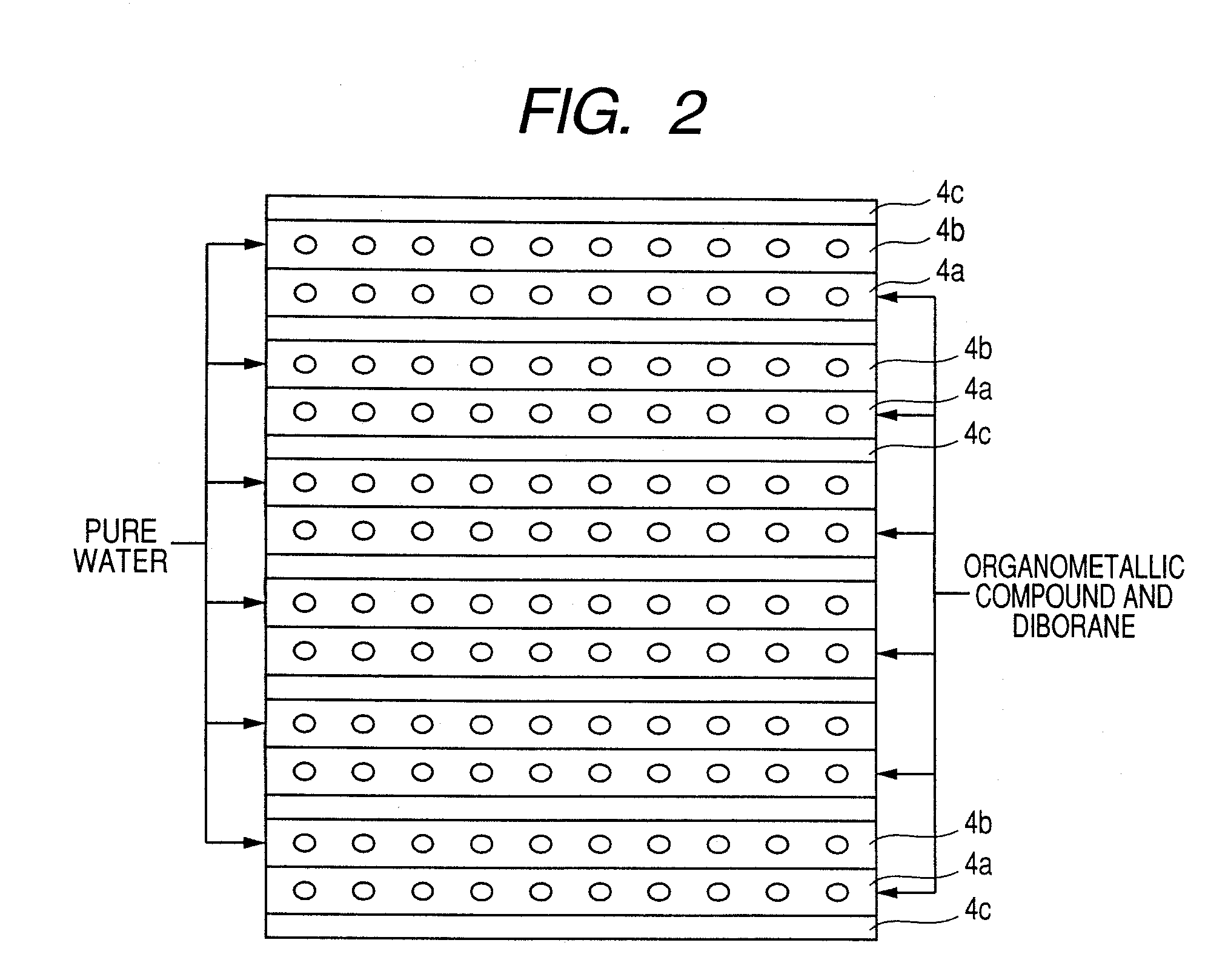
[0025]The invention provides a film deposition apparatus for continuously forming a multilayered transparent conductive film comprising a multilayered n-type semiconductor on a substrate and a method of the formation thereof. As shown in FIG. 1, this apparatus comprises a substrate attachment part 2 where a substrate A is attached to a setter 7a in the air, a charging part 3 where evacuation is conducted, a multilayer deposition treatment part 4 comprising two or more deposition treatment parts (41 to 4n) for forming a transparent conductive film comprising an n-type semiconductor (e.g., ZnO) on the heated substrate by the metal-organic chemical vapor deposition (MOCVD) method by reacting an organometallic compound (e.g., diethylzinc, Zn(C2H5)2), diborane (B2H6), and water (water vapor) in a vapor phase while heating the substrate, a takeout part 5 where the substrate having the multilayered transparent conductive film is discharged into the air (the pressure is returned to the atmo...


PUM

PropertyMeasurementUnit
temperaturesaaaaaaaaaa
transparentaaaaaaaaaa
transparent conductiveaaaaaaaaaa

Abstract

Raw materials are economized and a film deposition rate is improved while maintaining film evenness and high film quality.A film deposition apparatus for the continuous formation of a multilayered transparent conductive film is provided which comprises a substrate attachment part, a charging part where evacuation is conducted, a multilayer deposition treatment part comprising two or more deposition treatment parts for forming a transparent conductive film on a substrate by the MOCVD method by reacting an organometallic compound (diethylzinc), diborane, and water in a vapor phase, a substrate takeout part, a substrate detachment part, and a setter return part where the substrate setter is returned to the substrate attachment part. Film deposition is successively conducted while moving a substrate sequentially through the parts to form a multilayered transparent conductive film on the substrate. Each deposition treatment part is equipped with nozzles for spraying the organometallic compound, diborane, and water and with a cooling mechanism for cooling the nozzles.

Description

TECHNICAL FIELD[0001]The present invention relates to film deposition apparatus and a method of film formation for continuously forming a transparent conductive film having a multilayer structure by the MOCVD method.BACKGROUND ART[0002]The sputtering method and the metal-organic chemical vapor deposition (MOCVD) method are used in the step of forming a transparent conductive film among solar cell production steps. Reactions in the MOCVD method proceed at low temperatures (200° C. or lower) and it is a chemical vapor deposition method. Because of these, the MOCVD method is a mild film deposition technique which causes no mechanical damage to other thin constituent layers unlike the techniques in which the bombardment of energy particles damages underlying thin constituent layers, such as the sputtering method.[0003]In producing a CIGS type thin-film solar cell, a transparent conductive film is formed over thin constituent layers on the light incidence side thereof. The transparent co...

Claims


Application Information

Patent Timeline
Patent Type & Authority Applications(United States)
IPC IPC(8): H01L21/365C23C16/54
CPCC23C16/407C23C16/45572C23C16/45574C23C16/45578H01L21/0262H01L31/1884Y02E10/541H01L21/02554H01L21/02576C23C16/54Y02E10/549C23C16/40H01L31/04C23C16/455H10K30/00
Inventor TANAKA, YOSHIAKI
Owner SHOWA SHELL SEKIYU KK
Why Eureka
Try Eureka