Optical field receiver, optical multilevel signal receiver, and optical transmission system

Inactive Publication Date: 2009-08-20
HITACHI LTD
View PDF4 Cites 48 Cited by
  • Summary
  • Abstract
  • Description
  • Claims
  • Application Information

AI Technical Summary

Problems solved by technology

However, an implementation example in a field of the optical communication has not yet been reported.
As described above, although various arrangements of the signal points of the multilevel signal are reviewed from the past, the receiver becomes complicated as the number of multilevel increases.
Further, if the number of multilevel increases, an inter-symbol interference in optical delayed demodulation for demodulating phase components increases, resulting in a problem that characteristics, such as receiver sensitivity, are rapidly degraded.
If the modulation speed is increased as described above, however, signal quality is significantly degraded due to the chromatic dispersion in the optical fiber or fiber non-linear effects, such as self-phase modulation.
However, the tunable chromatic dispersion compensator has many problems to be solved, such as the size, complexity, cost, control

Method used


Image

  • Optical field receiver, optical multilevel signal receiver, and optical transmission system
  • Optical field receiver, optical multilevel signal receiver, and optical transmission system
  • Optical field receiver, optical multilevel signal receiver, and optical transmission system

Examples


first embodiment

[0053]FIG. 5 shows a first embodiment of an optical field receiver 100 according to the present invention. In FIG. 5, a path of an optical signal is represented by a thick line and a path of an electric signal is represented by a thin line.

[0054]An input optical signal 101 represented by equation r(n)exp(φ(n)) is branched into two optical signals by an optical branching circuit 102, likewise the decision-feedback type multilevel phase modulation receiver according to the prior art described in FIG. 4, to input to optical delayed demodulators 104-1 and 104-2. The optical delayed demodulators 104-1 and 104-2 include a first optical path that imparts a delay of a symbol time T to the input signal and a second optical path that has a phase shifter having a phase angle of 0 or π / 2 so that the phases in two demodulators deviate by π / 2 from each other, thereby to interfere a state (symbol) of the phase shifted optical multilevel signal with a symbol received previously by time T.

[0055]The ...

second embodiment

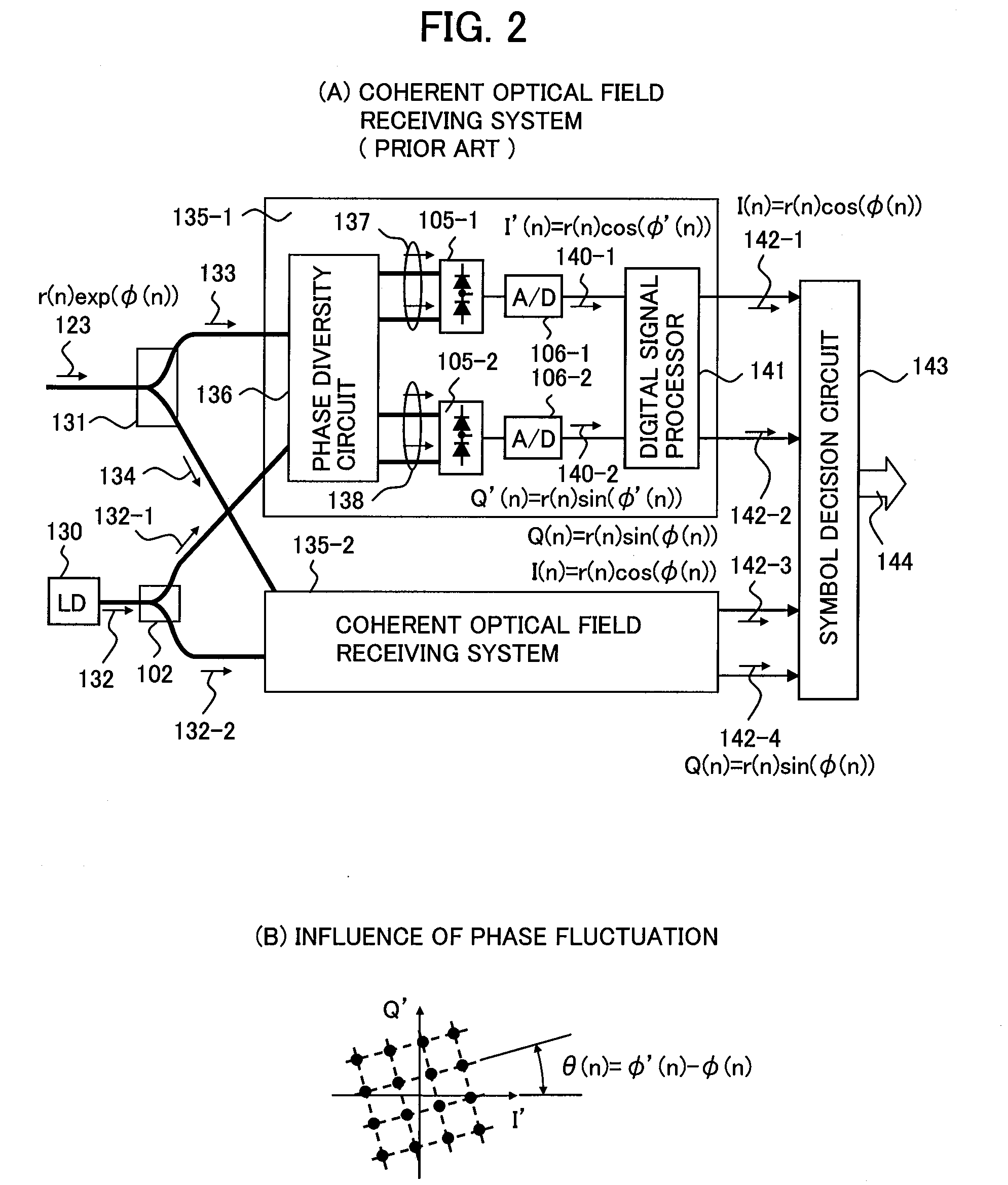
[0070]FIG. 8 is a second embodiment of the present invention and shows an optical multilevel signal receiver using the optical field receiver 100 shown in FIG. 5. When noise occurs in a transmission laser or an optical amplifier, these noises (for example, phase fluctuation) become a fluctuation factor of the optical field phase reconstructed in the optical field receiver. When optical multilevel signal 123 including the phase fluctuation θ(n) is received, the second embodiment can eliminate the influence of the phase fluctuation θ(n) from the reconstructed multilevel digital signal.

[0071]The received optical multilevel signal 123 is processed in the optical field receiver that includes the optical branching circuit 102, the optical delayed demodulators 104 (104-1 and 104-2), the balanced optical receivers 105 (105-1 and 105-2), the A / D converters 106 (106-1 and 106-2), the delay adjusting circuits 108 (108-1 and 108-2), and the field processing unit 111, which is the same as the co...

third embodiment

[0088]FIG. 11 is a third embodiment of the optical field receiver of the present invention and shows the optical multilevel signal receiver of the configuration that adds the optical intensity receiving function and the clock extraction function.

[0089]In the third embodiment, the input optical multilevel signal 123 is divided into three optical signals in the optical branching circuit 150. The first and second optical signals are input to the optical delayed demodulators 104-1 and 104-2, respectively and the third optical signal is input to the optical intensity receiver 151. The outputs of the optical delayed detectors 104-1 and 104-2 are converted into electric signals in the balanced optical receivers 105 (105-1 and 105-2), such as in FIG. 8, and then supplied to the field processing unit 111 via the A / D converters 106 (106-1 and 106-2) and the delay adjusting circuits 108 (108-1 and 108-2). The output signal of the optical intensity receiver 151 is converted into the digital sig...


PUM


Abstract

An optical field receiver comprises an optical branching circuit for branching a received optical multilevel signal into first and second optical signals, a first optical delayed demodulator for performing delayed demodulation on the first optical signal at a delay time T (T=symbol time), a second optical delayed demodulator for performing delayed demodulation on the second optical signal at the delay time T with an optical phase difference deviating from the first optical delayed demodulator by 90°, first and second optical receivers for converting each of the delayed demodulation signals representing x and y components of complex signals output from the first and second delayed demodulators into first and second electrical signals, and a field processing unit fort generating a first reconstructed signal representing an inter-symbol phase difference or a phase angle of a received symbol from the first and second electrical signals for each symbol time T.

Description

TECHNICAL FIELD[0001]The present invention relates to an optical information transmission technology, and more specifically, to an optical field receiver suitable for receiving optical multilevel signal transmitted over an optical fiber, an optical multilevel signal receiver, and an optical transmission system.BACKGROUND ART[0002]In recent years, even though the quantity of information (transmission capacity) transmittable over one optical fiber continues to increase as the number of multiplexed wavelength channels increases and the modulation speed of an optical signal becomes faster and faster. The increase of the transmission capacity reaches a limit of approximately 10 T (Tera)bit / s. The main reason why it is difficult to increase the transmission capacity is that a wavelength bandwidth usable for the optical transmission reaches the maximum bandwidth of a wavelength bandwidth (a sum of C-band, L-band, and S-band corresponds to approximately 80 nm=10 THz) of an optical fiber amp...

Claims


Application Information

Patent Timeline
IPC IPC(8): H04B10/12H04B10/06H04B10/516G02F2/00H04B10/2507H04B10/556H04B10/58H04B10/61H04J14/00H04J14/02
CPCH04B10/69H04B10/672H04L7/0008H04L7/0075
Inventor KIKUCHI, NOBUHIKO
Owner HITACHI LTD
Why Eureka
Try Eureka