Sensing Chip

a technology of sensing chip and sensor, which is applied in the field of photoelectron integration, can solve the problems of inability to adjust, low detection sensitivity, and inability to universalize and apply, and achieves the effects of high detection sensitivity, high precision, and reduced sample liquid

Active Publication Date: 2009-08-20
ROHM CO LTD +1
View PDF3 Cites 16 Cited by
  • Summary
  • Abstract
  • Description
  • Claims
  • Application Information

AI Technical Summary

Benefits of technology

[0016]The present invention measures the refractive index through the long-range surface plasmon polariton and introduces a strip-like structure, the buffer layer and a reference arm as profitable effects, whereby the has three advantages. First, the change in the transmission loss or (and) the change in the light spot size is employed as the target of measurement in place of a spatial reflected light angle of the prior art, whereby an integratible dielectric refractive index measuring apparatus can be provided. Second, buffer layer 3 has a refractive index substantially identical to that of lower dielectric 4. Transmission loss caused by the difference between the refractive indices of lower dielectric 4 and the sample liquid can be reduced by comprising buffer layer 3. Therefore, the apparatus can sense an antigen-antibody reaction, SNPs, a gene-protein interaction, a cell / protein function, as well as a bio material and a biological reaction such as an associative function in high detection sensitivity. In addition, the buffer layer / metal structure is a structure effective for protecting the metal against damage from the liquid. Therefore, the apparatus can be used in a severer situation. In addition, this structure is suitable in relation to molecular modification. The buffer layer is so introduced that the measurement range and precision can be adjusted, and the refractive index of the liquid or an antigen-antibody reaction of an organism can be measured with high precision in a wide-ranging manner. Third, convenience is aimed at coupling an optical fiber and a light guide end face, chip sealing is supported by the reference arm, the long-range surface plasmon polariton is excited by the method of coupling the optical fiber and the light guide end face, a control portion for spatial incident light is omitted, a pigtail fiber can be sealed in an attached chip, and this is an invention having a more practical industrial value.

Problems solved by technology

This conventional measuring method requires separate components such as a prism and a turntable, and is hence hard to adjust due to a large size.
Further, the method is inferior in stability, and at a high cost.
Therefore, universalization and application thereof are extremely limited.
However, although this method is highly precise, the measurement range is small, and the structure thereof is not suitable to sealing and practical use, but exerts disadvantageous influence on universalization and application.

Method used


Image

  • Sensing Chip
  • Sensing Chip
  • Sensing Chip

Examples


example 1

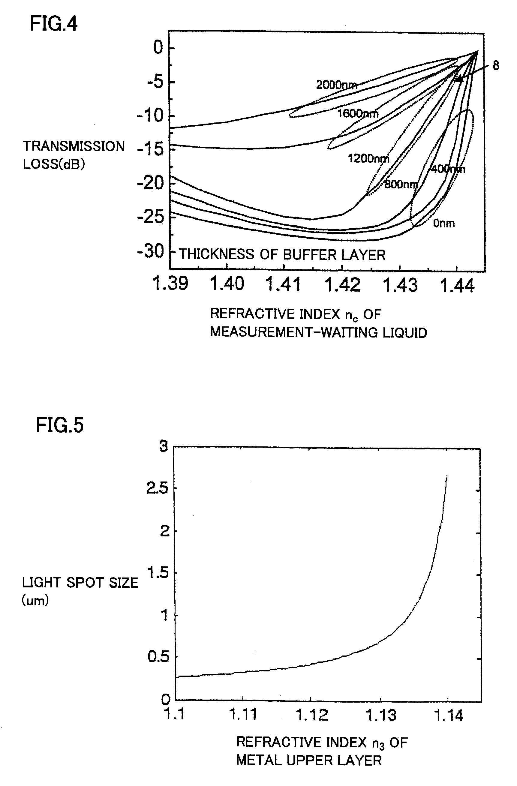
[0030]FIG. 6 is a diagram showing the basic structure of a sensing chip for a refractive index of a long-range surface plasmon polariton. FIG. 7 is an A-A sectional view of FIG. 6. FIG. 8 is a B-B sectional view of FIG. 6. FIG. 9 is a C-C sectional view of FIG. 6. An Si substrate (underlayer) 10 is selected. SiO2 or SiOx is selected as the material for a lower limiting layer 601 and an upper limiting layer 602, and lower limiting layer 601 is formed on Si substrate 10 by PECVD. A strip-like pattern of 81m in width is formed on lower limiting layer 601 by photolithography. Then, an Au thin film 603 of 20 nm in thickness is formed by sputtering or vapor deposition, and a measurement Au arm 21, a first reference Au arm 22 and a second reference Au arm 23 are formed by lifting or wet etching. Thereafter a buffer layer 604 made of SiOx or SiNy is formed by a method such as sputtering, vapor deposition or spin coater hardening. In response to specific measurement conditions, the thickness...

example 2

[0032]FIGS. 6, 7, 8 and 9 are diagrams showing the basic structure of Example 2 of a sensing chip of a long-range surface plasmon polariton for a refractive index. An Si substrate 10 is selected. SiO2 or SiOx (0≦x≦2) is selected as the material for a lower limiting layer 601 and an upper limiting layer 602, and lower limiting layer 601 is formed on Si substrate 10 by PECVD. A strip-like pattern of 8 μm in width is formed on lower limiting layer 601 by photolithography. Then, an Au thin film 603 of 20 nm in thickness is formed by sputtering or vapor deposition, and a measurement Au arm 21, a first reference Au arm 22 and a second reference Au arm 23 are formed by lifting or wet etching. Thereafter a buffer layer 604 made of SiOx or SiNy is formed by a method such as sputtering, vapor deposition or spin coater hardening.

[0033]In response to specific measurement conditions, the thickness of buffer layer 604 is set to 10 nm to 1 μm. Upper limiting layer 602 is formed by PECVD. Finally, ...

example 3

[0036]FIGS. 6, 7, 8 and 9 show the basic structure of Example 3 of a sensing chip for a refractive index of a long-range surface plasmon polariton. An Si substrate 10 is selected. BCB is selected as the material for a lower limiting layer 601 and an upper limiting layer 602, and lower limiting layer 601 is formed on Si substrate 10 by spin coater hardening. A strip-like pattern of 8 μm in width is formed on lower limiting layer 601 by photolithography. Then, an Au thin film 603 of 20 nm in thickness is formed by sputtering or vapor deposition, and a measurement Au arm 21, a first reference Au arm 22 and a second reference Au arm 23 are formed by lifting or wet etching. Thereafter a buffer layer 604 made of SiOx or SiNy is formed by a method such as sputtering, vapor deposition or spin coater hardening. In response to specific measurement conditions, the thickness of buffer layer 604 is set to 10 nm to 1 μm. Upper limiting layer 602 is formed by spin coater hardening. Finally, a meas...


PUM

PropertyMeasurementUnit
widthaaaaaaaaaa
thicknessaaaaaaaaaa
thicknessesaaaaaaaaaa

Abstract

There is provided a sensing chip capable of measuring a refractive index by utilizing a long-range surface plasmon polariton, accurately measuring an accumulative refractive index in a wide range, and more easily enabling sealing for measurement. The present invention relates to the sensing chip which has a thin metal film or a strip-like metal grown on an underlayer, and has a dielectric that limits a refractive index and a dielectric buffer layer on an upper surface and a lower surface of the thin metal film or the strip-like metal. The dielectric buffer layer is attached onto the thin metal film or the strip-like metal. The thin metal film or the strip-like metal and the buffer layer are sandwiched between two dielectric layers. A hole is made in a surface of the upper dielectric layer to serve as a measurement groove.

Description

BACKGROUND OF THE INVENTION[0001]1. Field of the Invention[0002]The present invention relates to the photoelectron integration technical field, and more particularly, it relates to a sensing (measurement) chip for a refractive index of a long-range surface plasmon polariton applied in the region of photon integration, a sensor and the like.[0003]2. Description of the Background Art[0004]A surface plasmon polariton ((SPP), FIG. 1) is an electromagnetic field transmitted along the interface between a metal and a dielectric, and the amplitude thereof is exponentially attenuated in the dielectric in response to the distance from the interface. The SPP is a kind of surface wave whose electromagnetic field energy is concentrated in the vicinity of the interface between the metal and the dielectric, and hence the electromagnetic field on the metal surface is strong and extremely sensitive to the mode of the surface, particularly a change in the refractive index. Thus, the SPP is widely app...

Claims


Application Information

Patent Timeline
Patent Type & Authority Applications(United States)
IPC IPC(8): C12M1/34G01N21/41
CPCG01N21/41G01N21/7703G01N21/553
Inventor DONG, HUANG YIYI, RAOFANG, LIUWEI, ZHANGDE, PENG JIANGOHNISHI, DAINIWA, DAISUKETAZUKE, ATSUSHIMIURA, YOSHIKATSU
Owner ROHM CO LTD
Why Eureka
Try Eureka