Temperature and pressure control methods to fill features with programmable resistance and switching devices

a technology of programmable resistance and switching device, which is applied in the direction of bulk negative resistance effect device, semiconductor device, electrical apparatus, etc., can solve the problems of reducing the material density of the material, limiting the goal of device miniaturization, and increasing the difficulty of processing the device, so as to reduce structural irregularities, increase the surface mobility, and increase the effect of material density

Active Publication Date: 2009-09-10
OVONYX MEMORY TECH LLC
View PDF3 Cites 8 Cited by
  • Summary
  • Abstract
  • Description
  • Claims
  • Application Information

AI Technical Summary

Benefits of technology

[0027]In accordance with one embodiment of the instant invention, a programmable resistance material or switching material deposition is performed using conventional deposition processes in addition to increasing surface mobility within the active material layer to uniformly cover the insulative layer and to fill the insulative layer opening to the conductive bottom electrode layer with an active material layer. Uniform covering the insulative layer with the active material layer and filling the active material within the opening reduces structural irregularities within the opening thereby increasing material density, reducing thickness variations in the active material layer, reducing device shunting and early failure of the device, and improving device characteristics.

Problems solved by technology

One of the significant practical challenges that the programmable resistance memory and switching devices face is to reduce the contact area of one or more electrodes contacting the chalcogenide material.
Lithography is commonly used to define small-scale features of semiconductor devices and often sets a limit on the goal of device miniaturization.
As the feature size of devices is minimized, however, processing of the devices becomes more difficult.
Small scale features become more difficult to define as the lithographic limit of resolution is reached and features that are defined become more difficult to process.
As the dimension or length scale of an opening decreases upon miniaturization, it becomes increasingly difficult to satisfactorily fill the opening with another material.
Techniques such as physical vapor deposition (PVD) or sputtering fail to provide dense or complete filling of openings when the dimensions of the opening are reduced below a critical size.
Instead of providing a dense, uniform filling, these techniques increasingly incompletely fill openings as the dimension of the opening decreases while the depth stays the same, thus increasing the aspect ratio.
Lack of structural uniformity in the filling of openings compromises device functionality as variations occur from device-to-device across an array of devices on a substrate.
In addition, less than optimal performance is achieved for each device due to the defective nature of the deposited material.
Deep, narrow channels, for example, are more difficult to uniformly fill than channels that are shallow and wide.
With deep, narrow features, sputtering and other physical deposition techniques are oftentimes unable to deliver sufficient material uniformly to underlying layers, to the bottom of the feature or to completely fill an opening within the device.
Poor opening filling can lead to uncontrolled thickness variation of the active material, leading to device shunting, premature device failure or poor device characteristics.
Conformality of deposition is another processing difficulty that becomes exacerbated as feature size decreases.
In addition to difficulties with achieving uniform filling, openings also present complications for achieving conformal deposition that become more pronounced as size of the opening decreases.
Achieving conformality over discontinuous features becomes increasingly difficult as the feature size of the opening decreases or the aspect ratio of the opening increases.
The imperfections detract from device performance and reliability.
As illustrated in prior art FIGS. 1-2, the openings are typically very difficult to fill by standard PVD sputtering, evaporation, or other directional deposition processes without forming structural irregularities.
Although CVD in principle is a viable strategy for filling lithographic or sublithographic openings in programmable resistance and switching devices, the technique is limited in practice because of the unavailability of gas phase precursors for a variety of desirable programmable resistance, fast switching, and other contact materials.
In addition, the reaction conditions (e.g. high temperatures or plasma conditions) needed to react the precursors may damage other layers in the device structure.
Also, CVD deposition methods often require complex chemistries which result in unwanted additional atomic elements being incorporated at undesirably high levels in the deposited film.

Method used


Image

  • Temperature and pressure control methods to fill features with programmable resistance and switching devices
  • Temperature and pressure control methods to fill features with programmable resistance and switching devices
  • Temperature and pressure control methods to fill features with programmable resistance and switching devices

Examples


Embodiment Construction

[0041]The making and using of the presently preferred embodiments are discussed in detail below. It should be appreciated, however, that the present invention provides many applicable inventive concepts that can be embodied in a wide variety of specific contexts. The specific embodiments discussed are merely illustrative of specific ways to make and use the invention, and do not limit the scope of the invention.

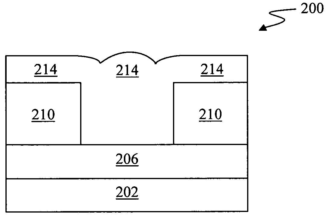
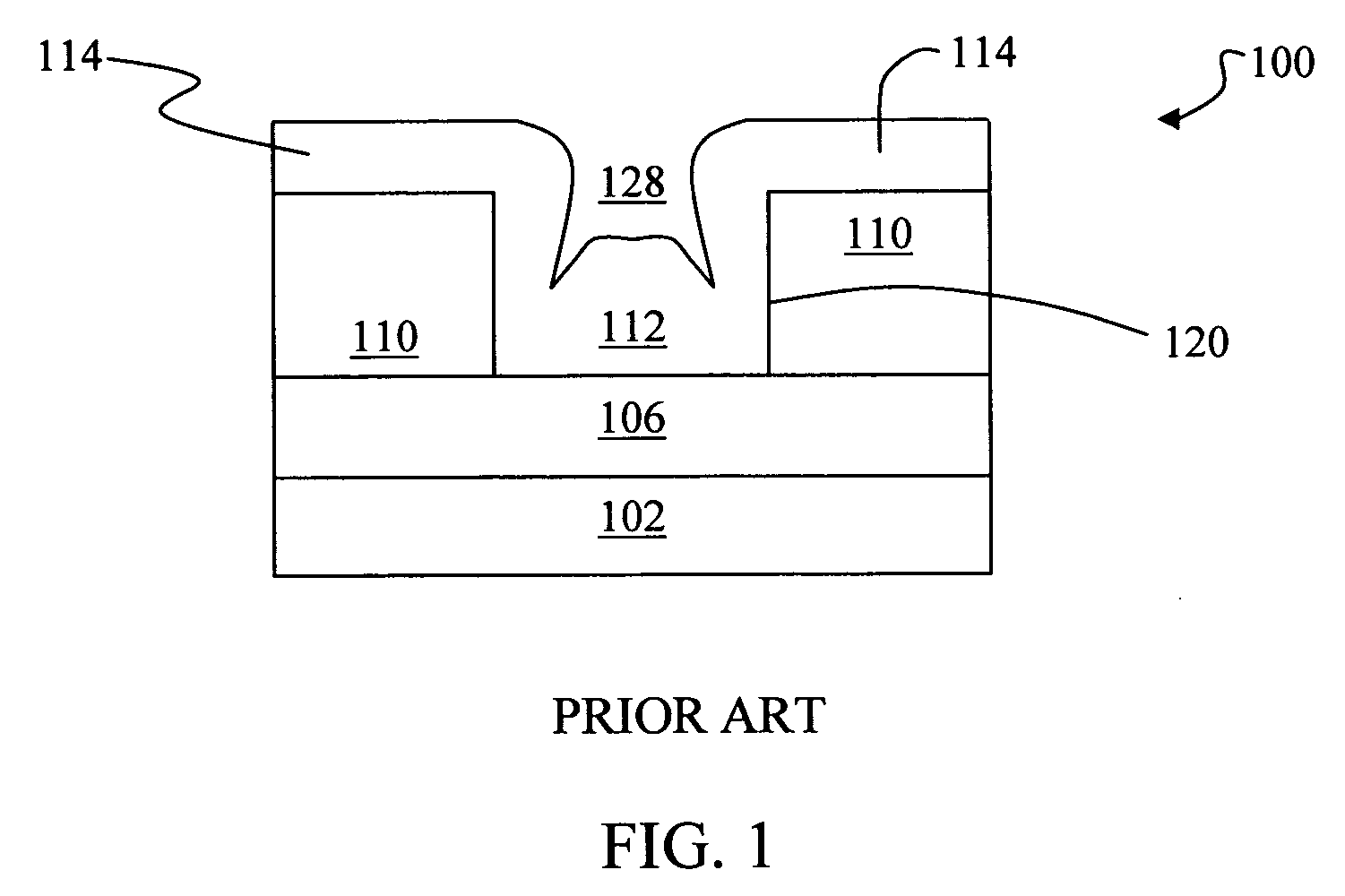
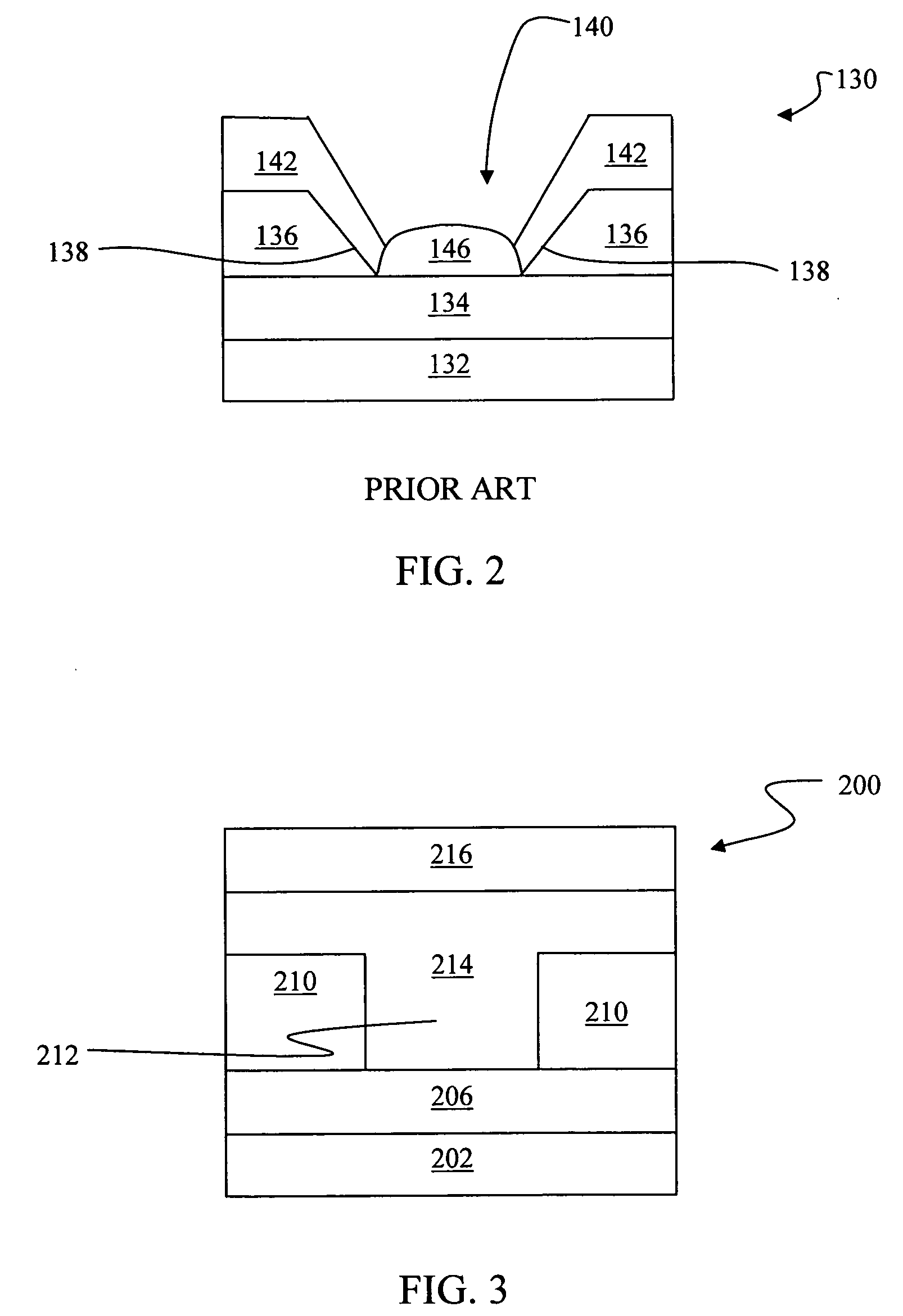
[0042]The intermediate stages of manufacturing a novel electronic device including conformally filling openings within an insulating material in accordance with the instant invention are illustrated in FIGS. 1 through 9. Throughout the various views and illustrative embodiments of the instant invention, like reference numbers are used to designate like elements.

[0043]The instant invention improves uniformity and conformal coverage of a conventional deposition process and helps prevent the problem of structural irregularities occurring during deposition processes including phy...


PUM


Abstract

A programmable resistance, chalcogenide, switching or phase-change material device includes a substrate with a plurality of stacked layers including a conducting bottom electrode layer, an insulative layer having an opening formed therein, an active material layer deposited over both the insulative layer, within the opening, and over selected portions of the bottom electrode, and a top electrode layer deposited over the active material layer. The device uses temperature and pressure control methods to increase surface mobility in an active material layer, thus providing complete coverage or fill of the openings in the insulative layer, selected exposed portions of the bottom electrode layer, and the insulative layer.

Description

FIELD OF INVENTION[0001]This invention relates generally to uniform and complete filling of openings within programmable resistance and switching devices having one or more electrical contacts. More particularly, this invention relates to forming programmable resistance and switching device structures with active materials that uniformly cover intermediate layers and openings within the device. Most particularly, this invention relates to temperature and pressure control methods used to form programmable resistance and switching devices with uniform layers and openings having reduced structural irregularities, improved filling, uniform film thickness and improved device characteristics.BACKGROUND OF THE INVENTION[0002]Programmable resistance materials and fast switching materials are two classes of promising active materials for next-generation electronic storage, computing and signal transfer devices. A programmable resistance material possesses two or more states that differ in el...

Claims


Application Information

Patent Timeline
Patent Type & Authority Applications(United States)
IPC IPC(8): H01L47/00
CPCH01L45/06H01L45/1233H01L45/1641H01L45/1625H01L45/144H10N70/231H10N70/041H10N70/026H10N70/8828H10N70/826
Inventor FOURNIER, JEFFCZUBATYJ, WOLODYMYRLOWREY, TYLER
Owner OVONYX MEMORY TECH LLC
Why Eureka
Try Eureka