Ion source, ion beam processing/observation apparatus, charged particle beam apparatus, and method for observing cross section of sample

a cross-sectional and sample technology, applied in the field of ion source, ion beam processing/observation apparatus, charged particle beam apparatus, can solve the problems of complex structure of the device, difficult control, spatial interference between nearby lenses, etc., and achieve the effect of reducing the amount of time and high flatness

Active Publication Date: 2009-09-17
HITACHI HIGH-TECH CORP
View PDF11 Cites 89 Cited by
  • Summary
  • Abstract
  • Description
  • Claims
  • Application Information

AI Technical Summary

Benefits of technology

[0013]In view of the foregoing problems, it is, therefore, an object of the present invention to provide an ion beam machining and observation method relevant to a technique of cross sectional observation of an electronic component, through which a sample is machined by using an ion beam withdrawn from the same ion source and one can observe a machined portion of the sample. Another object of the present invention is to provide a charged particle beam processor capable of reducing the time it takes to fill up a processed hole yet ensuring a high degree of flatness at a filled hole area.
[0016]Particularly, when the ion beam machining and observation device of the present invention irradiates a gas ion beam to process a sample, it projects a hole shape of an aperture mask inside an ion beam irradiation column into a sample shape, such that a high-speed machining can be possible.
[0017]Moreover, to reduce the amount of a sample being cut out at the time of cross sectional observation, the ion beam machining and observation device of the present invention includes a mechanism for mass-separating a gas ion beam emitted from an ion source, and executes a control operation to prevent an ion having a relatively large mass number from reaching the sample when it irradiates an ion having a relatively small mass number.
[0040]Therefore, the ion beam machining and observation technique according to the present invention can be advantageously used for observing a cross section of an electronic component such as semiconductor devices including a semiconductor memory, a microprocessor, a semiconductor laser, etc., and a magnetic head, by using ion beams extracted from the same ion source to process a sample and to observe a machined portion of the sample. Moreover, the present invention technique is capable of reducing the amount of time it takes to fill up a processed hole, while ensuring a high degree of flatness at a filled hole area.

Problems solved by technology

Therefore, a device thereof has a complicated structure and is difficult to control.
This consequently causes device prices to increase.
Spatial interference between nearby lenses is another problem as they are positioned to let ion beam and electron beam irradiate the same spot on a sample.
This problem cannot be resolved without suffering from performance degradation of each beam.
However, if the same kind of ion used for machining is used for observation again, the sample surface is cut away, making it difficult to observe a desired cross section of the sample.
Unfortunately, a new technique for sample machining and observation by ion beam has not been developed yet.
Meanwhile, because the hole fill volume is a large value at an equivalent level to the processed hole volume, it takes a long period of time (from several minutes to several tens of minutes) to fill up the hole, and the amount of time it takes to return the wafer to a production line occupies a large portion of a series of processes.

Method used


Image

  • Ion source, ion beam processing/observation apparatus, charged particle beam apparatus, and method for observing cross section of sample
  • Ion source, ion beam processing/observation apparatus, charged particle beam apparatus, and method for observing cross section of sample
  • Ion source, ion beam processing/observation apparatus, charged particle beam apparatus, and method for observing cross section of sample

Examples


embodiment 1

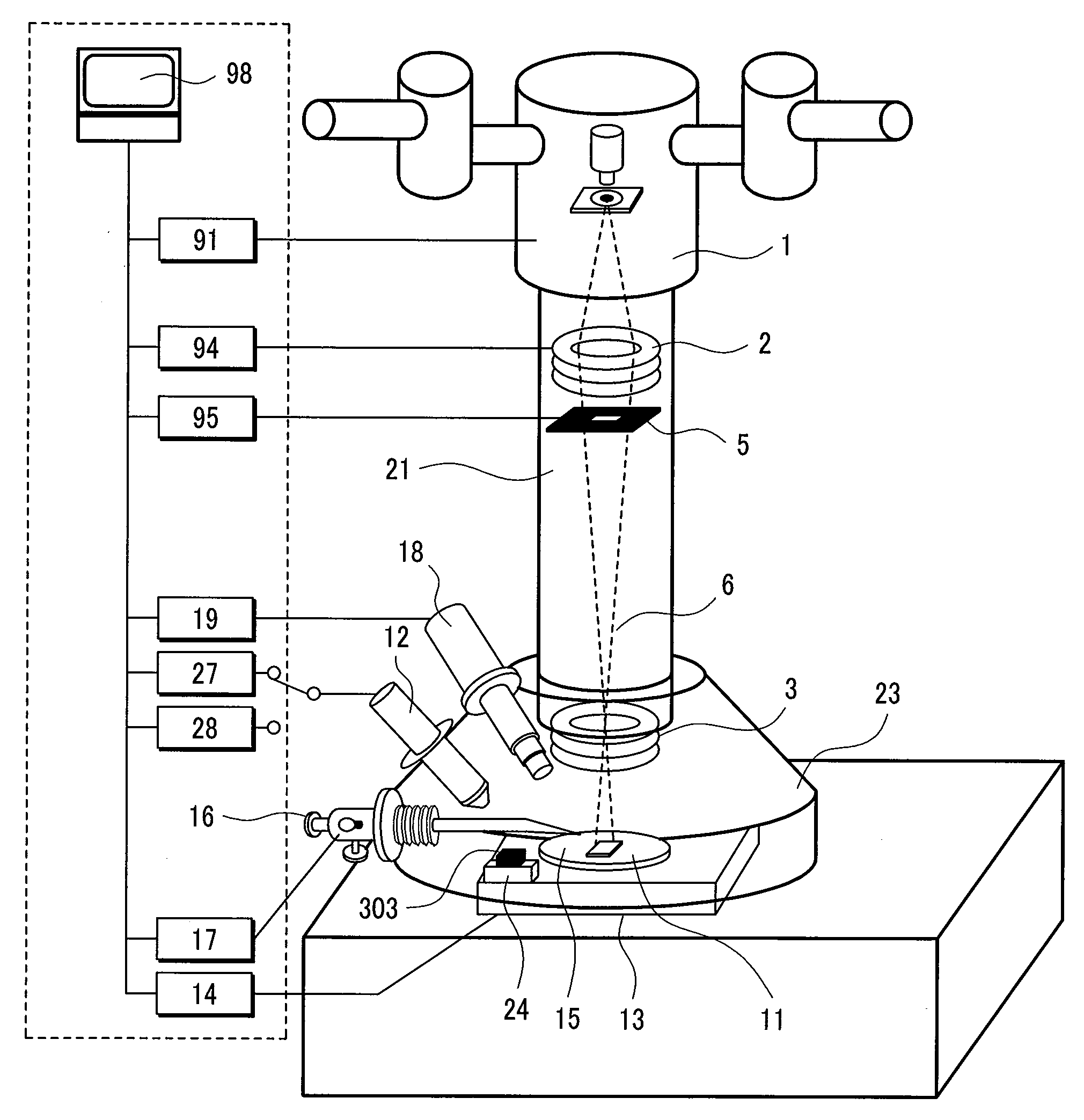
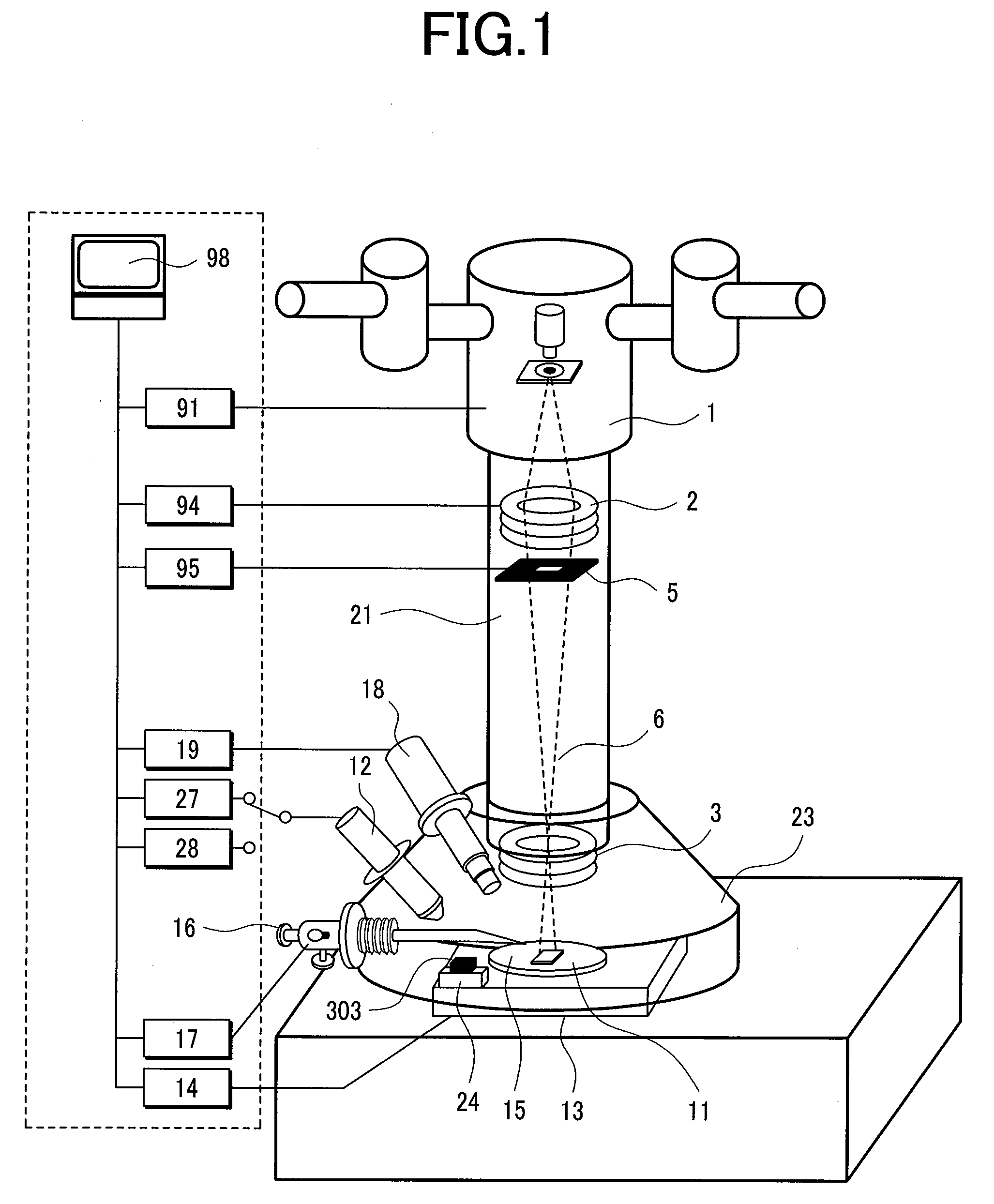
[0087]FIG. 1 illustrates an ion beam machining and observation device according to one embodiment of the present invention. Particularly, the device of this embodiment is capable of irradiating two kinds of gas ions onto a sample by using a duoplasmatron 1 as a plasma ion source. In general, brightness of the plasma ion source is lower than brightness of a liquid metal ion source such as Ga by at least 2 to 3 orders of magnitude. Therefore, in case of this embodiment a stencil mask 5 having a predetermined shape aperture is inserted into the mid course of an ion beam irradiation system inside an ion beam column 21, and the aperture shape is projected onto a sample to obtain a projected beam for use. Preferably, inert gases or the kind of an element like oxygen and nitrogen may be chosen as the kind of the ion for the ion source such that electrical properties of a device are not affected thereby, and defects are much less likely to occur even when a completely machined wafer by usin...

embodiment 2

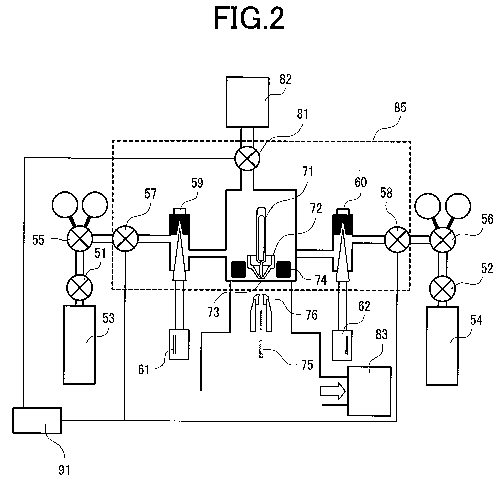
[0109]Unlike the ion beam machining and observation device discussed in Embodiment 1 where ion beam irradiation systems are arranged in a perpendicular direction, an ion beam machining and observation device of this embodiment has ion beam irradiation systems arranged in a direction inclined from the perpendicular direction, and a stage plane is fixed in a horizontal direction.

[0110]Moreover, the device of this embodiment includes a mass divider installed midway in the ion beam path to get rid of ions of large mass numbers when ions of relatively small mass numbers are irradiated.

[0111]This embodiment will also explain a means for preparing a TEM (Transmission Electron Microscope) sample by extracting a micro sample from a sample.

[0112]This embodiment also uses a mask aperture shaped ion beam projected on a sample.

[0113]FIG. 4 illustrates an ion beam machining and observation device of this embodiment. The ion beam machining and observation device includes a duoplasmatron 1, which i...

embodiment 3

[0149]FIG. 9 illustrates an embodiment of using a gas field ion source as an ion source. The configuration of the gas supply mechanism of this embodiment is identical to that of the system explained in Embodiment 1. Therefore, the description on its operation will be omitted in this embodiment.

[0150]In this ion source, the apex of an ion emitter tip 402 made of tungsten is machined sharply and cooled to several tens of K by a freezer 401. A gas is also cooled and a strong electric field is applied to the ion emitter tip 402, to thereby extract an ion beam from near the emitter tip.

[0151]In case of extracting helium ions or hydrogen ions, as shown in FIG. 10, a nano-pyramid structure 404 of an atom is formed at an ion emitter tip apex 403. Since ions are produced only near one through three atoms, an ion source with a very high brightness is realized. That is, an ion beam 405 of 1 nm or less in diameter is obtained on a sample, the sample can be observed at very high spatial resoluti...


PUM

PropertyMeasurementUnit
voltageaaaaaaaaaa
voltageaaaaaaaaaa
currentaaaaaaaaaa

Abstract

An ion beam machining and observation method relevant to a technique of cross sectional observation of an electronic component, through which a sample is machined by using an ion beam and a charged particle beam processor capable of reducing the time it takes to fill up a processed hole with a high degree of flatness at the filled area. The observation device is capable of switching the kind of gas ion beam used for machining a sample with the kind of a gas ion beam used for observing the sample. To implement the switch between the kind of a gas ion beam used for sample machining and the kind of a gas ion beam used for sample observation, at least two gas introduction systems are used, each system having a gas cylinder a gas tube, a gas volume control valve, and a stop valve.

Description

CLAIM OF PRIORITY[0001]The present invention claims priority from Japanese application JP 2007-113358 filed on Apr. 23, 2007 and JP 2007-161691 filed on Jun. 19, 2007, the contents of which are hereby incorporated by reference into this application.BACKGROUND OF THE INVENTION[0002]The present invention relates to an inspection and analysis technique for use in an electronic component such as semiconductor devices including a semiconductor memory, a microprocessor, a semiconductor laser, etc., and as a magnetic head; and, more particularly, to a technique of machining (or processing) and observation of the cross section of a sample by an ion beam.[0003]High manufacturing yield is an important requisite for the manufacture of electronic components, such as semiconductor devices, e.g., semiconductor memories typically represented as dynamic random access memories (DRAMs), microprocessors and semiconductor lasers, and magnetic heads. This is because a fall of the product yield is direct...

Claims


Application Information

Patent Timeline
Patent Type & Authority Applications(United States)
IPC IPC(8): H01J49/26H01J27/02
CPCH01J27/10H01J37/08H01J37/28H01J37/3023H01J37/3056H01J2237/006C23C14/3442H01J2237/0807H01J2237/0825H01J2237/0827H01J2237/31745H01J2237/31749H01J2237/057
Inventor SHICHI, HIROYASUTOMIMATSU, SATOSHIUMEMURA, KAORUKANEOKA, NORIYUKIISHIGURO, KOJI
Owner HITACHI HIGH-TECH CORP
Why Eureka
Try Eureka