
Sensor device

a technology of sensor device and sensor body, which is applied in the direction of photovoltaics, fluid speed measurement using thermal variables, volume/mass flow by thermal effects, etc., can solve the problem that the device is not suitable for an aircraft in service, and achieve the effect of reducing the heat loss from the element to the surrounding parts

Active Publication Date: 2009-09-17
BAE SYSTEMS PLC
View PDF6 Cites 10 Cited by
  • Summary
  • Abstract
  • Description
  • Claims
  • Application Information

AI Technical Summary

Benefits of technology

[0004]It is an object of the invention to provide a sensor device made with microfabrication techniques having a heated sensor element wherein heat loss from the element to surrounding parts is reduced.
[0006]The concept of the invention is to provide a sensor device fabricated by techniques of microfabrication (in the art, such techniques are generally referred to as MEMS technology). A heating element is formed as a resistive film or layer that may be exposed to a hazardous environment, and is for example mounted flush with the surface of an aircraft's fuselage. Electrical connections to the heating (resistive) element are made through a substrate on which the heating element is mounted, to the rear side of the substrate. In order to reduce heat loss from the element to the adjacent parts of the device, and to maintain sensitivity of the device, the following measures are involved:
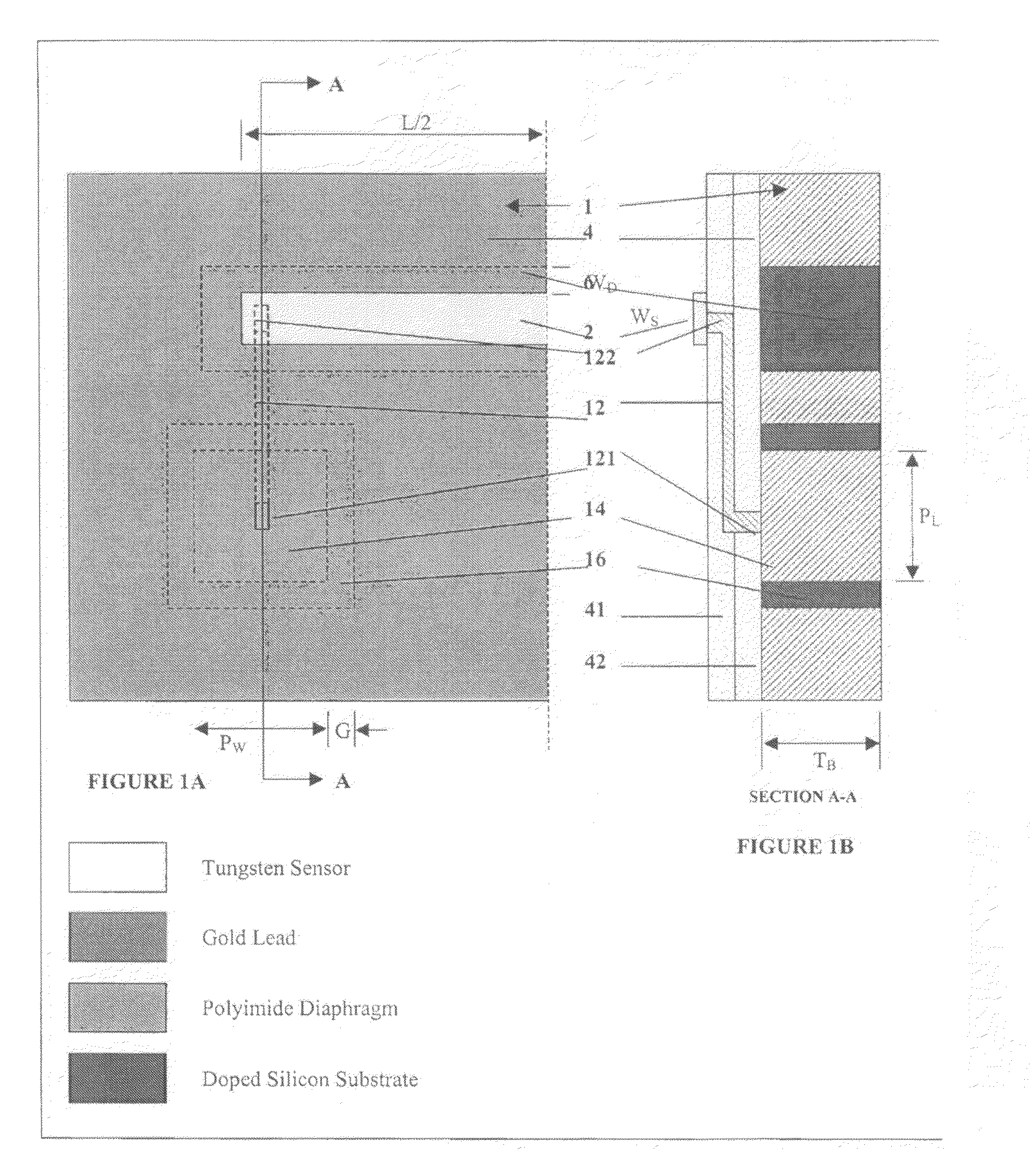
[0023]At least in a preferred embodiment, the sensor is a rectangular sensing element, comprising a film of Tungsten, supported on a 6 μm thickness silicon oxide / polyimide / silicon oxide diaphragm to reduce heat losses to the substrate. Reliable electrical connections to the back side of the sensor are addressed using a novel interconnect system. Heat loss is further reduced as the interconnects are thermally isolated from the substrate. The leads running from the sensing element are buried between the diaphragm layers to improve robustness and reduce lead convective losses. This has resulted in a significant improvement in performance. Sensitivity is increased to 950 mV / Pa and frequency response is increased to at least 20 kHz. Substantial reductions in parasitic resistance have allowed power consumption per device to be less than 10 mW under static conditions rising to around 350 mW at a free stream velocity of 240 m / s. The flexible layout of the design coupled with a common device footprint allowed a range of integration methods to be evaluated along with a variety of sensor element configurations.
[0024]The sensor element preferably for simplicity in manufacture has constant width along its entire length. Alternatively the sensor width may be varied such that the width is greater in the centre than at the ends. The purpose of this variable width resistor is to obtain a constant temperature distribution along the sensor element. This reduces the maximum temperature on the sensing element for a given overall resistance—giving the potential to operate at a greater overheat ratio if required. Results have suggested that, for a typical sensor operating at a maximum local temperature of 340° C. (probably somewhat greater than actual operating temperatures), distributing the sensor platform area to achieve a roughly constant temperature distribution gave about 30° C. reduction in maximum local temperature. There is also an additional slight improvement in sensor and diaphragm convection characteristics.
[0026]The polyimide layer in the diaphragm should be as thin as possible. It significantly reduces heat flow to the substrate and increases convective losses both from the sensor and polyimide (with a marginally greater proportional effect on the sensor than on the diaphragm). Increasing diaphragm width reduces the heat flow to the substrate. Additionally, it increases the convection from the sensor and, to a greater proportion, from the diaphragm. Therefore, increasing diaphragm width will increase the overall sensitivity of the device (through increased sensor and diaphragm convection) but may reduce the frequency response of the device since a greater proportion of the overall convection is from the thermally ‘sluggish’ polyimide diaphragm.

Problems solved by technology

However such devices are not suitable for an aircraft in service, since they are fragile.

Method used


Image

  • Sensor device
  • Sensor device
  • Sensor device

Examples


third embodiment

Device Build

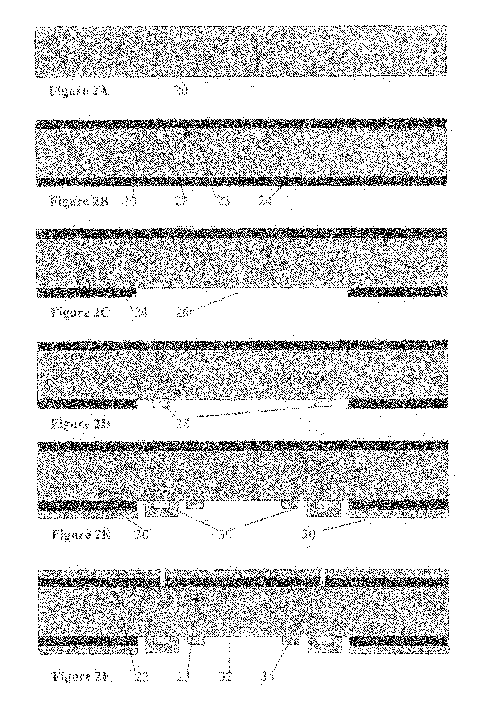
[0084]The fabrication sequence was modified in the light of the above, and the third embodiment is shown in FIG. 8 as the following sequence: Similar parts to those of FIG. 2 are denoted by the same reference numeral.

[0085]FIG. 8A Silicon wafer 20 250 μm thick, heavily doped with As-resistivity 0.0001-0.004 ohm cm is provided.

[0086]FIG. 8B Deposit 0.3 μm silicon oxide film 24 on rear face only.

[0087]FIG. 8C Etch oxide layer 24 on reverse to expose silicon substrate as at 26.

[0088]FIG. 8D Deposit a 0.3 μm tungsten adhesion / diffusion barrier layer 80, followed by a 0.5 μm gold layer 81 on exposed silicon substrate 26. Etch to form back contacts 28.

[0089]FIG. 8E Deposit 0.1 μm tungsten, etch to form top ohmic contacts 82, To improve conductivity, the tungsten layer was deposited on the top side of the wafer prior to any other processing on this face, i.e. before any significant contamination could be introduced. The tungsten layer was patterned to give 400 μm square contact...


PUM


Abstract

A sensor device for sensing air flow speed at the exterior of an aircraft, comprising a substrate having an upper side on which is mounted a diaphragm over an aperture or recess in the substrate, the diaphragm being thermally and electrically insulative, and mounting on its upper surface a heating element comprising a layer of resistive material, and wherein electrical connections to the heating element are buried in the diaphragm and / or the substrate, and provide electrical terminals at the lower side of the substrate. The heating element is exposed to the environment, but the remaining electrical parts of the device are not exposed.

Description

FIELD OF THE INVENTION[0001]The present invention relates to a sensor device and a method of making a sensor device, employing techniques of microfabrication, and particularly though not exclusively, a sensor device employing a heated element for sensing a variable such as aircraft wind speed.BACKGROUND OF THE INVENTION[0002]Anemometry devices for measuring wind speed by exposure of an electrically heated element to air flow are known. For example devices have been used in wind tunnels comprising a wire suspended between upstanding terminals. The wire is electrically energised and is mounted in a bridge circuit to monitor changes of resistance arising from changes in temperature of the element (via the temperature coefficient of resistance) when the wind speed changes. However such devices are not suitable for an aircraft in service, since they are fragile. In order to measure the wind speed of an aircraft, a device is required that is resistant to knocks and abrasions.[0003]It has ...

Claims


Application Information

Patent Timeline
Patent Type & Authority Applications(United States)
IPC IPC(8): H01L29/66H01L21/50
CPCG01P5/12G01F1/6845G01P13/025
Inventor WARSOP, CLYDEPRESS, ANDREW JULIANHUCKER, MARTYN JOHN
Owner BAE SYSTEMS PLC
Learn More