Method for Forming Resist Pattern, Method for Producing Circuit Board, and Circuit Board

a technology of resist pattern and resist pattern, which is applied in the direction of resist details, photomechanical equipment, instruments, etc., can solve the problems of difficult to form all wiring patterns, high production cost, and difficult quality management, and achieve accurate forming, stable method of forming, and simplified steps

Inactive Publication Date: 2009-09-24
MITSUBISHI PAPER MILLS LTD +1
View PDF2 Cites 17 Cited by
  • Summary
  • Abstract
  • Description
  • Claims
  • Application Information

AI Technical Summary

Benefits of technology

[0032]In the method for forming a resist pattern (1) according to the present invention, a resin layer and a mask layer are provided on one surface (first surface) of a substrate having a through-hole(s) to plug the through-hole(s), and the resin layer on the through-hole(s) and on a periphery of the through-hole(s) is removed by a resin layer removing solution supplied from the opposite surface (second surface).
[0033]The resin layer removing solution supplied from the second surface passes through the through-hole(s) and reaches the resin layer on the first surface to dissolve and to remove the resin layer on the through-hole(s) and on the periphery of the through-hole(s). The mask layer is composed of a component insoluble in the resin layer removing solution. Accordingly, the resin layer removing solution can accurately remove only the resin layer on the through-hole(s) and on the periphery of the through-hole(s) precisely and selectively. Therefore, the resin layer can be extremely accurately formed with the substrate uncovered only on the through-hole(s) and on the periphery of the through-hole(s), and a landless or small-land-width pattern can be easily formed by the subsequent step.
[0034]In the method for forming a resist pattern (2) according to the present invention, the resin layer and the mask layer are integrally formed, so that the steps can be simplified. An extremely stable method for forming a resist pattern can be simply realized by previously forming a film having the resin layer and the mask layer stacked, and forming the film integrally with the substrate by a means such as lamination.
[0035]In the method for forming a resist pattern (3) according to the present invention, the resin layer is a photocrosslinkable resin layer. Accordingly, not only is the resin layer on the through-hole(s) and on the periphery of the through-hole(s) removed, but also a resist pattern can be formed on the surface of the substrate by pattern exposure, and the subsequent step of forming a circuit pattern on the through-hole(s) and the surface of the substrate can be simply performed.
[0036]In the method for forming a resist pattern (4) according to the present invention, the substrate having a through-hole(s) is an insulating substrate having a conductive layer on the surface and on the inner wall of a through-hole(s). Therefore, it is possible to form a resist pattern for forming a more reliable circuit board.
[0037]In the method for producing a circuit board (5) according to the present invention, a photocrosslinkable resin layer and a mask layer are formed on a first su...

Problems solved by technology

The method is advantageous for forming a fine circuit; however, since all conductive layers are formed by electroless plating, the production cost is high, disadvantageously.
However, it is difficult to form all wiring patterns with a uniform thickness by electrolytic plating, and quality management is difficult, disadvantageously.
Since an image is weakened by side etching of a conductive layer, for example, the method has limitations as compared with the other two methods in terms of formation of a fine circuit.
When alignment is inaccurate, a hole and a land are not concentric circles, disadvantageously.
However, when the land width is small as shown in FIG. 55(a), if misalignment occurs by the same distance x during alignment of an exposure mask, a through-hole is placed out of a land, making it impossible to form a narrow land on the whole outer periphery of the through-hole, disadvantageously.
Actually, there are limitations to alignment accuracy due to forming hole accuracy, stretching of a substrate, a change in dimension of an exposure photomask, and the like.
Through-holes having various diameters are formed on a high-density circuit board, and the number of the holes is also extremely large.
Therefore, it is extremely difficult to perform accurate alignment for all through-holes.
Accordingly, although a landless or small-land-width through-hole is needed for a high-density circuit board, a small-land-width through-hole must be designed to have a large land width so that the through-hole is surely shielded and a negative (photocrosslinkable) dry film photoresist is not crosslinked, disadvantageously (e.g. Patent Document 2).
For this reason, it is difficult for a plating solution to enter the through-hole and plating is not performed, disadvantageously.
A positive (photodegradable) electrodeposition photoresist must be degraded by exposure; however, the inside of a columnar through-hole cannot be completely exposed.
Therefore, the electrodeposition photoresist in the through-hole cannot be completely degraded and cannot be used as a plating resist layer.
However, when the corner of a through-hole has a tapered shape, light...

Method used


Image

  • Method for Forming Resist Pattern, Method for Producing Circuit Board, and Circuit Board
  • Method for Forming Resist Pattern, Method for Producing Circuit Board, and Circuit Board
  • Method for Forming Resist Pattern, Method for Producing Circuit Board, and Circuit Board

Examples


example 1

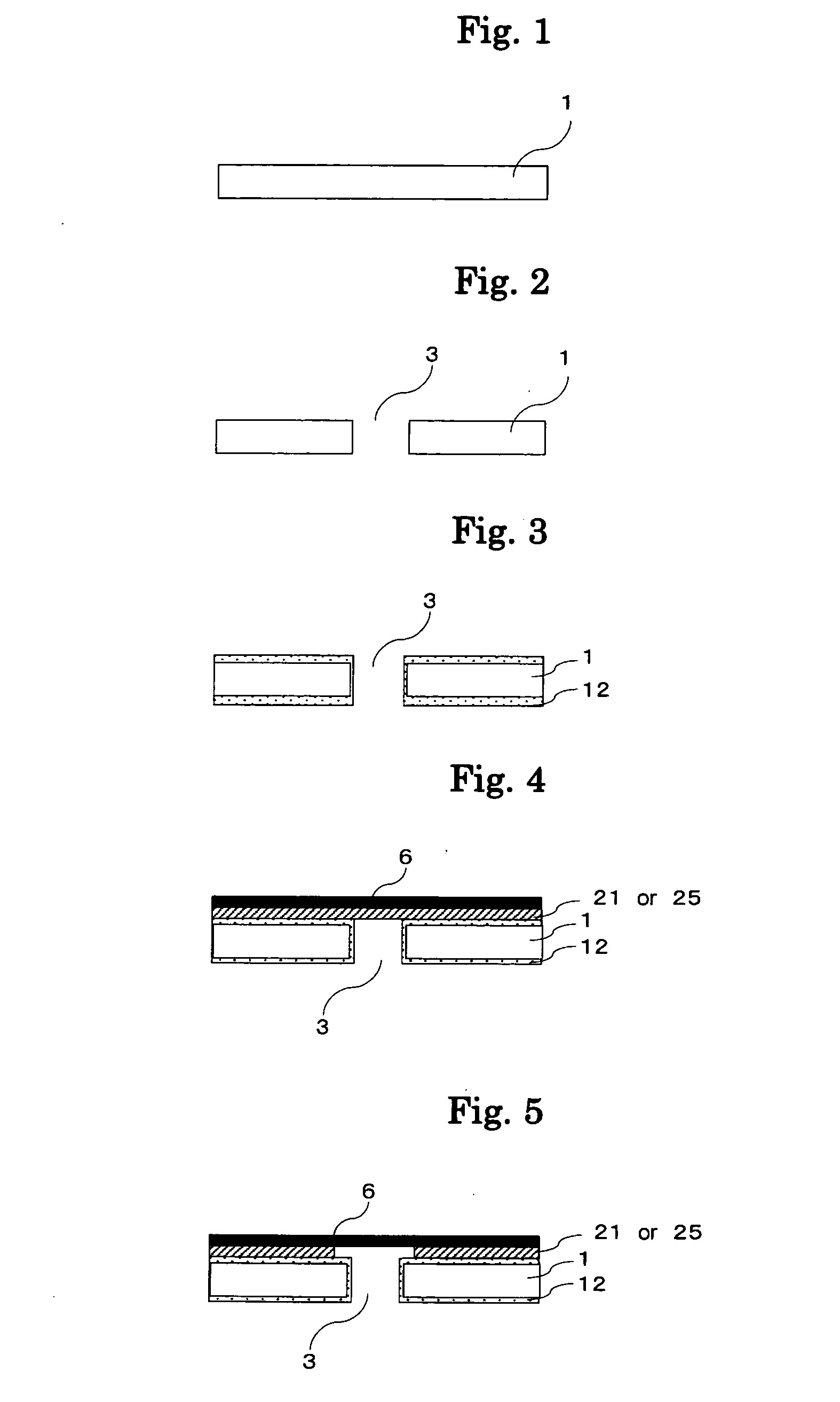
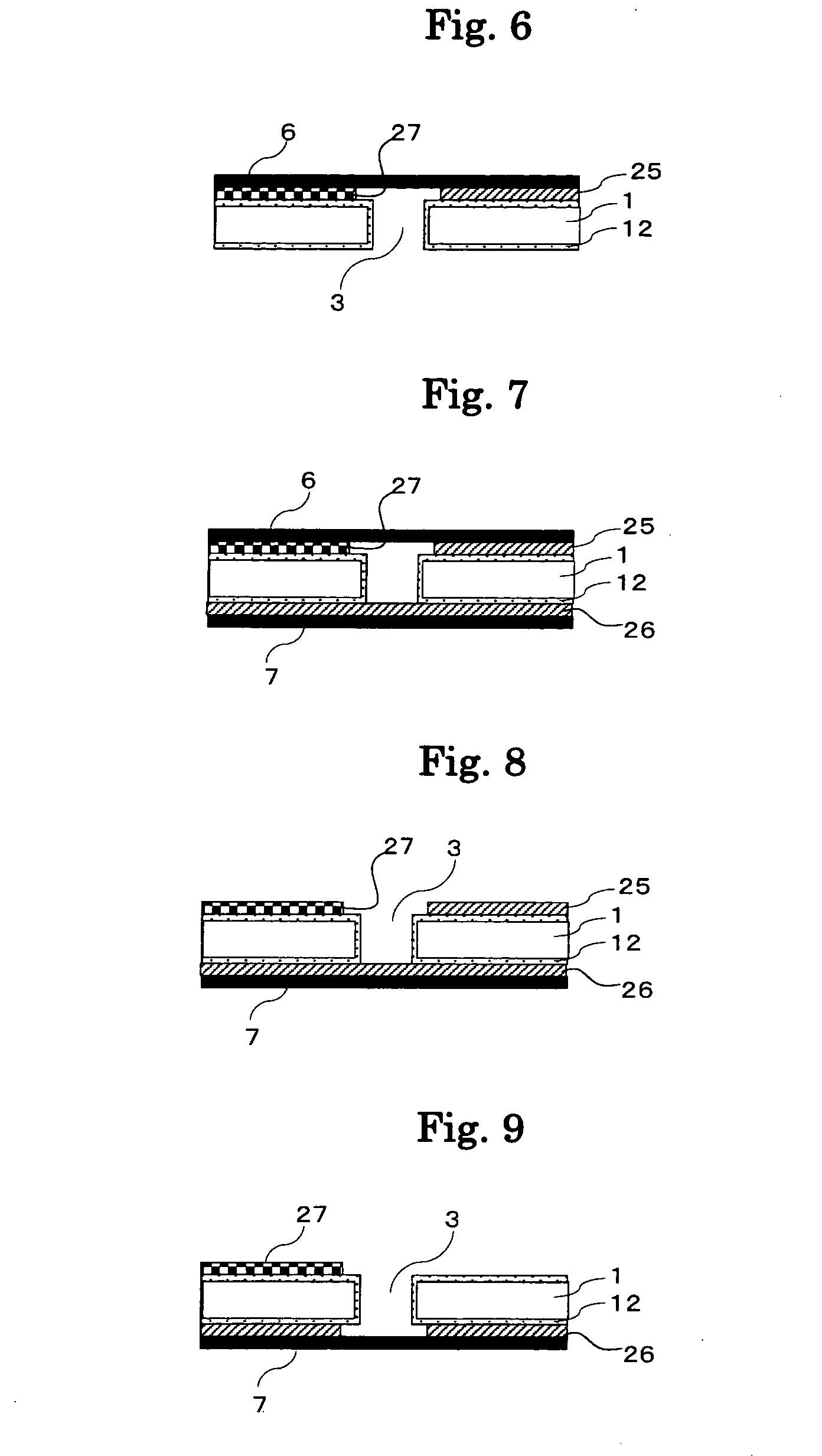
[0169]Through-holes having a diameter of 0.1 mm were opened on a glass base epoxy resin substrate (area: 340 mm×510 mm, base thickness: 0.1 mm) using a drilling machine. Then, the substrate was subjected to desmear treatment and then electrolessly plated to provide an electroless copper plating layer having a thickness of about 0.5 μm as a first conductive layer on the surface including the inner wall of the each through-hole. A dry film photoresist for forming a circuit which is composed of a 25 μm photocrosslinkable resin layer and a 12 μm mask layer (support film, material: polyester) was thermocompression bonded to one surface (first surface) of the substrate using a dry film photoresist laminator to provide the photocrosslinkable resin layer and the mask layer (support film).

[0170]Then, a shower spray was applied from a second surface of the substrate at a spray pressure of 0.2 MPa for 32 seconds using a removing solution of a 1 mass % aqueous sodium carbonate solution (30° C.)...

example 2

[0180]A circuit board was prepared in the same manner as in Example 1, except that the time for treatment with a removing solution of a 1 mass % aqueous sodium carbonate solution (30° C.) was shortened to 26 seconds for the first surface and 28 seconds for the second surface when the photocrosslinkable resin layer on the each through-hole and on the periphery of the each through-hole on the first surface and the second surface was dissolved and removed in Example 1.

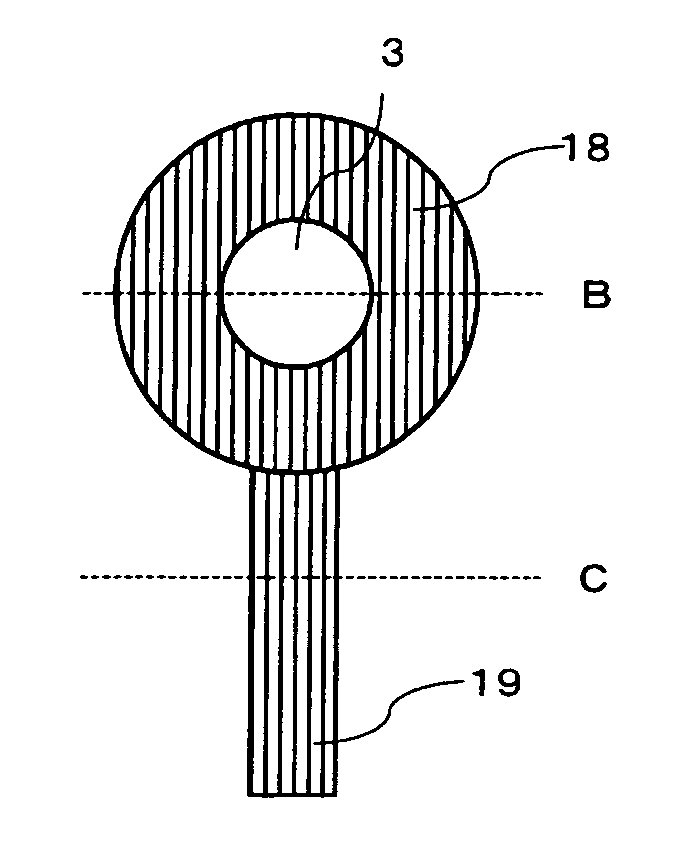
[0181]The each through-hole and the periphery of the each through-hole immediately before electrolytic copper plating were observed by an optical microscope for the first surface and the second surface, respectively, and it was found that the photocrosslinkable resin layer on the periphery of the each through-hole was removed concentrically with the each through-hole. The each through-hole diameter L1 when the hole was formed was 100 μm, the each through-hole diameter L2 when plated was 99 μm, the diameter L3 of the part ...

example 3

[0184]A circuit board was prepared in the same manner as in Example 1, except that the time for treatment with a removing solution of a 1 mass % aqueous sodium carbonate solution (30° C.) was extended to 50 seconds for both the first surface and the second surface when the photocrosslinkable resin layer on the each through-hole and on the periphery of the each through-hole on the first surface and the second surface was dissolved and removed in Example 1.

[0185]The each through-hole and the periphery of the each through-hole immediately before electrolytic copper plating were observed by an optical microscope for the first surface and the second surface, respectively, and it was found that the photocrosslinkable resin layer on the periphery of the each through-hole was removed concentrically with the each through-hole. The each through-hole diameter L1 when the hole was formed was 100 μm, the each through-hole diameter L2 when plated was 99 μm, the diameter L3 of the part from which ...


PUM


Abstract

There are provided a method for forming a resist pattern for preparing a circuit board having a landless or small-land-width through-hole(s) to realize a high-density circuit board, a method for producing a circuit board, and a circuit board. A method for forming a resist pattern, comprising the steps of forming a resin layer and a mask layer on a first surface of a substrate having a through-hole(s), and removing the resin layer on the through-hole(s) and on a periphery of the through-hole(s) on the first surface by supplying a resin layer removing solution from a second surface opposite to the first surface of the substrate, and a method for producing a circuit board using the method for forming a resist pattern, and a circuit board.

Description

TECHNICAL FIELD[0001]The present invention relates to a method for forming a resist pattern, a method for producing a circuit board, and a circuit board. More specifically, the present invention relates to a method for forming a landless or small-land-width resist pattern suitable for realizing a high-density circuit board and a fine wiring pattern on a circuit board, a method for producing a circuit board, and a circuit board.BACKGROUND ART[0002]As electronic equipment has been reduced in size and provided with multiple functions in recent years, a high-density circuit board and a fine wiring pattern on a circuit board have also been realized. A means for achieving such conditions is a multilayer circuit board. As shown in FIG. 45, in a circuit board formed by stacking multiple wiring layers, the layers are conducted to each other through a pore such as a through-hole or a non-through-hole (hereinafter collectively called “hole”) having an inner wall covered with a conductive layer...

Claims


Application Information

Patent Timeline
IPC IPC(8): H05K1/11G03F7/20
CPCH05K1/116H05K3/002H05K3/108H05K3/426H05K2203/1394H05K2203/0191H05K2203/0574H05K2203/1184H05K2201/09545
Inventor KANEDA, YASUOIRISAWA, MUNETOSHITOYODA, YUJIKOMURO, TOYOKAZUFUKASE, KATSUYASAKAI, TOYOAKI
Owner MITSUBISHI PAPER MILLS LTD
Why Eureka
Try Eureka