Method for manufacturing soi substrate

a technology of soi substrate and substrate layer, which is applied in the direction of semiconductor/solid-state device manufacturing, basic electric elements, electric apparatus, etc., can solve the problems of defects or damage of crystal defects, and deterioration of surface planarity, so as to reduce surface roughness, prevent defects or damage, and remove defects and damage of a surface

Active Publication Date: 2009-09-24
SEMICON ENERGY LAB CO LTD
View PDF51 Cites 35 Cited by
  • Summary
  • Abstract
  • Description
  • Claims
  • Application Information

AI Technical Summary

Benefits of technology

[0019]A single crystal semiconductor substrate is cleaved along a fragile region, and a single crystal semiconductor layer attached to a supporting substrate is subjected to first etching treatment and second etching treatment to remove defects and damage of a surface of the single crystal semiconductor layer and to reduce surface roughness of the single crystal semiconductor layer, and then, irradiated with laser light. Thus, defects or damage can be prevented from occurring in the single crystal semiconductor layer at the time of melting the single crystal semiconductor layer by the laser light irradiation. Accordingly, a

Problems solved by technology

However, due to an ion implantation step for forming the fragile region and a separation step, crystal defects remain on a surface of and in the silicon layer, and the planarity of the surface deteriorates.
In addition, there are problems such as a rough surface, variation in thickness, and minute chinks of the single crystal silicon layer if smooth cleavage for releasing the single crystal silicon layer is not conducted.
Removal of crystal defects of the semiconductor layer which is attached to a silicon wafer has been conventionally achieved by heating at a temperature of 1000° C. or higher; however, such a high temperature process cannot be utilized for removal of crystal defects of a semiconductor layer that is attached to a glass substrate having a strain point of 700° C. or lower.
That is, a conventional method has not been established by which the crystallinity of the single crystal semiconductor layer that is attached to the glass substrate having a strain point of 700° C. or lower is recovered to be the same level as or substantially the same level as that of a single crystal semiconductor substrate before being pro

Method used


Image

  • Method for manufacturing soi substrate
  • Method for manufacturing soi substrate
  • Method for manufacturing soi substrate

Examples


embodiment 1

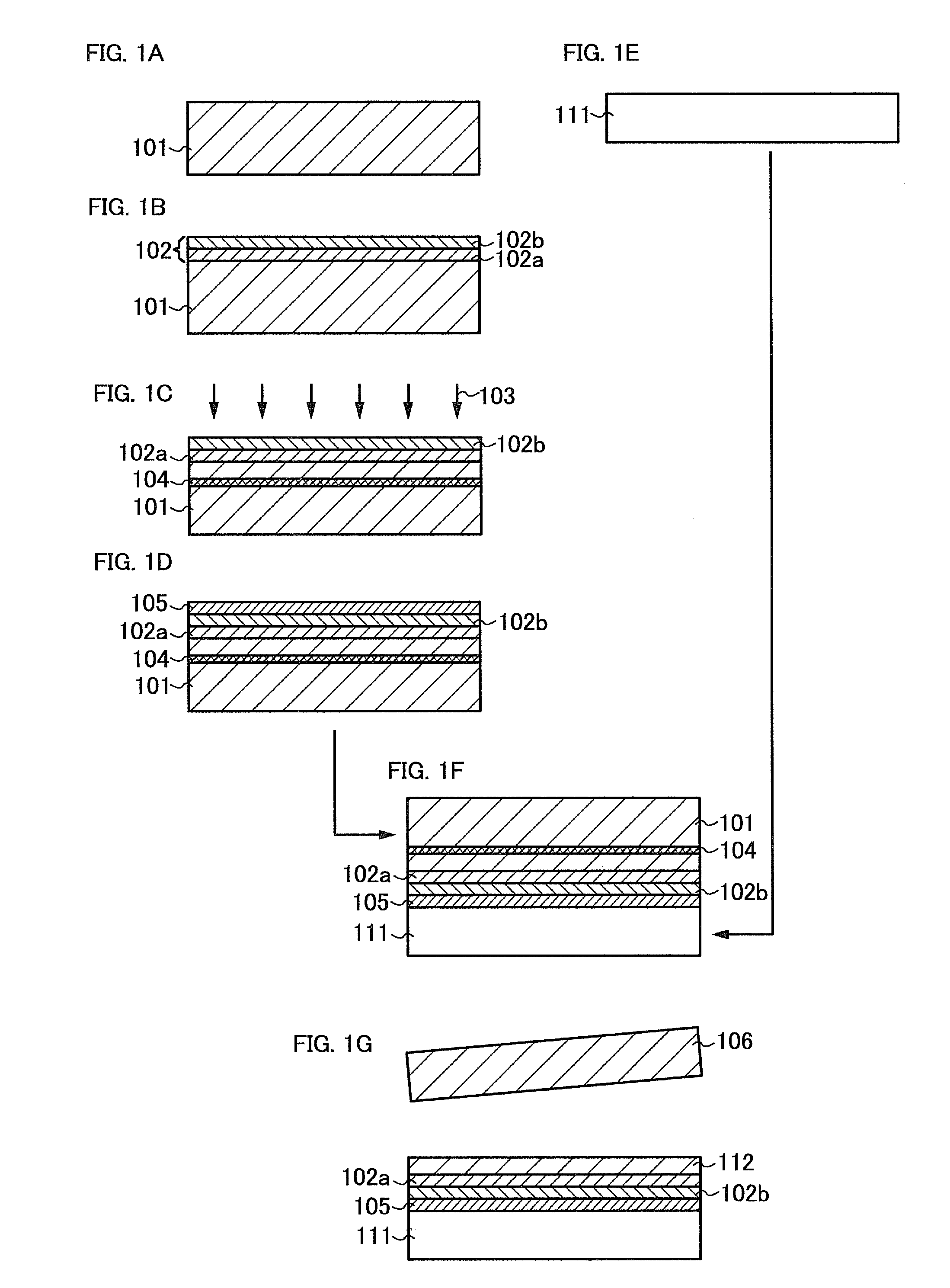
[0036]A method for manufacturing an SOI substrate will now be described with reference to drawings in this embodiment. In the method, a single crystal semiconductor substrate is cleaved to be separated into a single crystal semiconductor layer which is attached to a supporting substrate and a single crystal semiconductor substrate, and a surface of the single crystal semiconductor layer which is attached to the supporting substrate is subjected to first etching treatment and second etching treatment, and then irradiated with laser light. Further, this embodiment also describes a method for manufacturing an SOI substrate, an object of which is to provide a single crystal semiconductor layer for a substrate with a low upper temperature limit, such as a glass substrate.

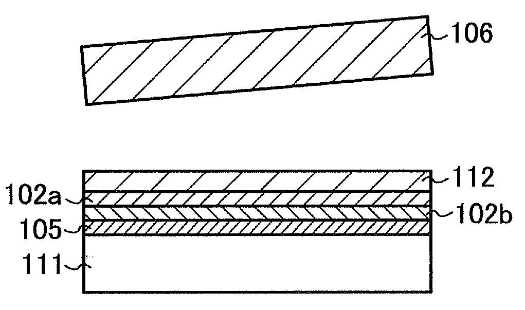
[0037]First, a single crystal semiconductor substrate 101 is prepared (see FIG. 1A). The single crystal semiconductor substrate 101 is processed into a desired size and shape. The single crystal semiconductor substrate 1...

embodiment 2

[0095]A structure of an SOI substrate which is different from the structure of the SOI substrate described in Embodiment 1 will now be described in this embodiment. Note that in this embodiment, the same reference numerals denote the same parts as in Embodiment 1, and a detailed description is omitted.

[0096]A structure in which the single crystal semiconductor layer 112 is formed over the supporting substrate 111 with the insulating film 102b and the insulating film 102a interposed therebetween is illustrated in FIG. 4. First, the insulating film 102a is formed over the single crystal semiconductor substrate 101. Then, the fragile region 104 is formed in the single crystal semiconductor substrate 101 by ion beam irradiation. Then, the insulating film 102b which serves as a bonding layer is formed over the insulating film 102a. After the insulating film 102b is formed, the single crystal semiconductor substrate 101 and the supporting substrate 111 are attached with the insulating fil...

embodiment 3

[0112]In this embodiment, a method for manufacturing a complementary metal oxide semiconductor (CMOS) is described with reference to FIGS. 7A to 7E and FIGS. 8A to 8D as an example of a method for manufacturing a semiconductor device including a high performance and highly reliable semiconductor element, with high yield. Note that repeated description for the like portions or portions having like functions to the portions in Embodiments 1 and 2 are omitted.

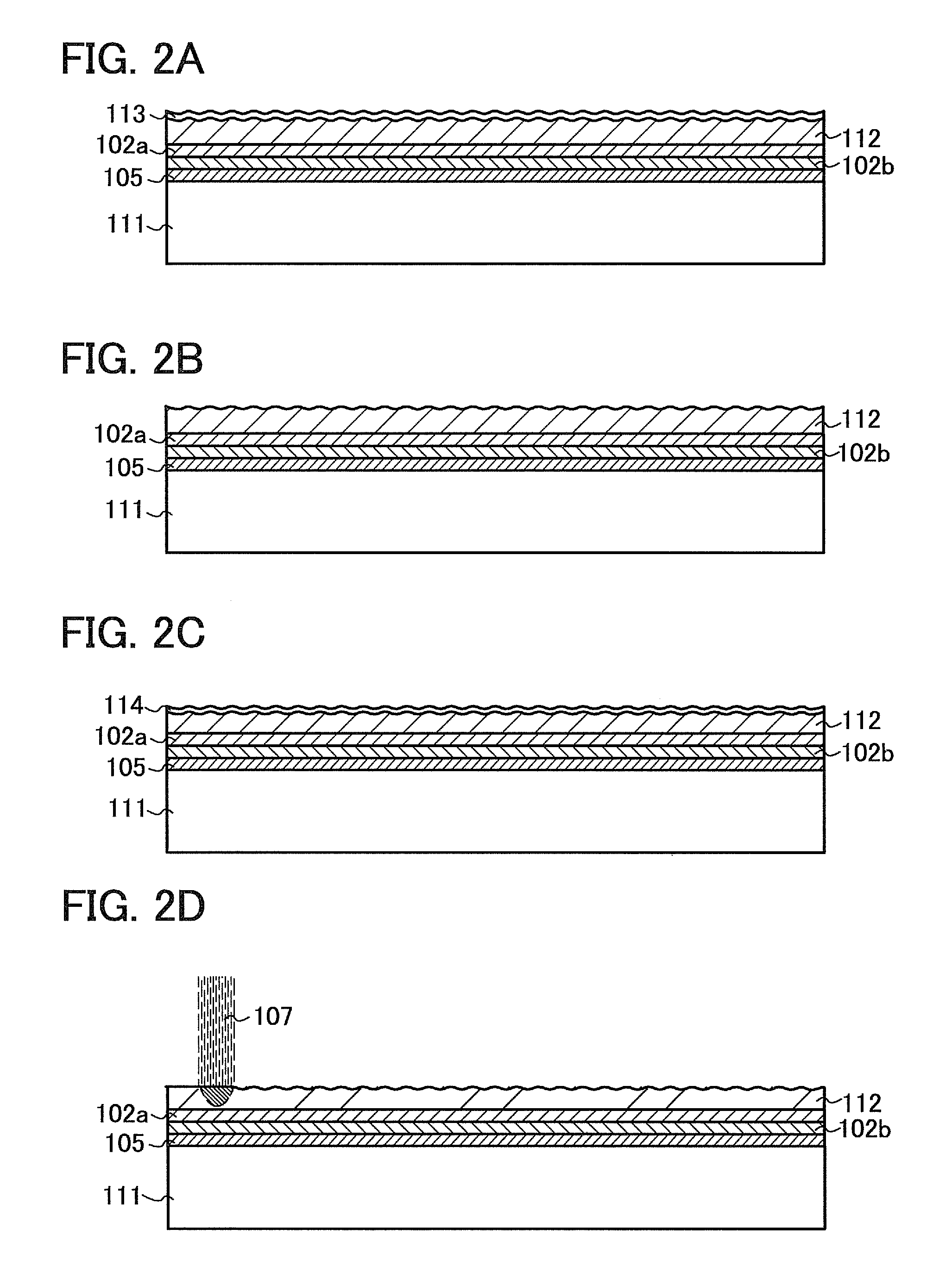
[0113]In FIG. 7A, the insulating film 102 and the single crystal semiconductor layer 112 are formed over the supporting substrate 111. Note that, although an example in which the SOI substrate having the structure illustrated in FIG. 4 is used is described here, an SOI substrate having another structure described in this specification can be used.

[0114]The single crystal semiconductor layer 112 is separated from the single crystal semiconductor substrate 101 and is subjected to planarization treatment. The planarization treatment ...


PUM


Abstract

Forming an insulating film on a surface of the single crystal semiconductor substrate, forming a fragile region in the single crystal semiconductor substrate by irradiating the single crystal semiconductor substrate with an ion beam through the insulating film, forming a bonding layer over the insulating film, bonding a supporting substrate to the single crystal semiconductor substrate by interposing the bonding layer between the supporting substrate and the single crystal semiconductor substrate, dividing the single crystal semiconductor substrate at the fragile region to separate the single crystal semiconductor substrate into a single crystal semiconductor layer attached to the supporting substrate, performing first dry etching treatment on a part of the fragile region remaining on the single crystal semiconductor layer, performing second dry etching treatment on a surface of the single crystal semiconductor layer subjected to the first etching treatment, and irradiating the single crystal semiconductor layer with laser light.

Description

BACKGROUND OF THE INVENTION[0001]1. Field of the Invention[0002]The present invention relates to a method for manufacturing an SOI substrate having a so-called silicon-on-insulator (SOI) structure in which a single crystal semiconductor layer is provided on an insulating surface, and a method for manufacturing a semiconductor device having the SOI structure.[0003]2. Description of the Related Art[0004]Integrated circuits in which an SOI substrate called a silicon-on-insulator (hereinafter also referred to as “SOI”) having a thin single crystal semiconductor layer on an insulating surface is used instead of a silicon wafer which is manufactured by thinly slicing a single crystal semiconductor ingot have been developed. The integrated circuits using the SOI substrate have been attracting attention due to their reduced parasitic capacitance between a drain of a transistor and a substrate, which will lead to an improvement of semiconductor integrated circuits.[0005]As a method for manuf...

Claims


Application Information

Patent Timeline
IPC IPC(8): H01L21/762
CPCH01L21/76254
Inventor SUZAWA, HIDEOMISASAGAWA, SHINYASHIMOMURA, AKIHISAMOMO, JUNPEIKURATA, MOTOMUMURAOKA, TAIGANEI, KOSEI
Owner SEMICON ENERGY LAB CO LTD
Why Eureka
Try Eureka