

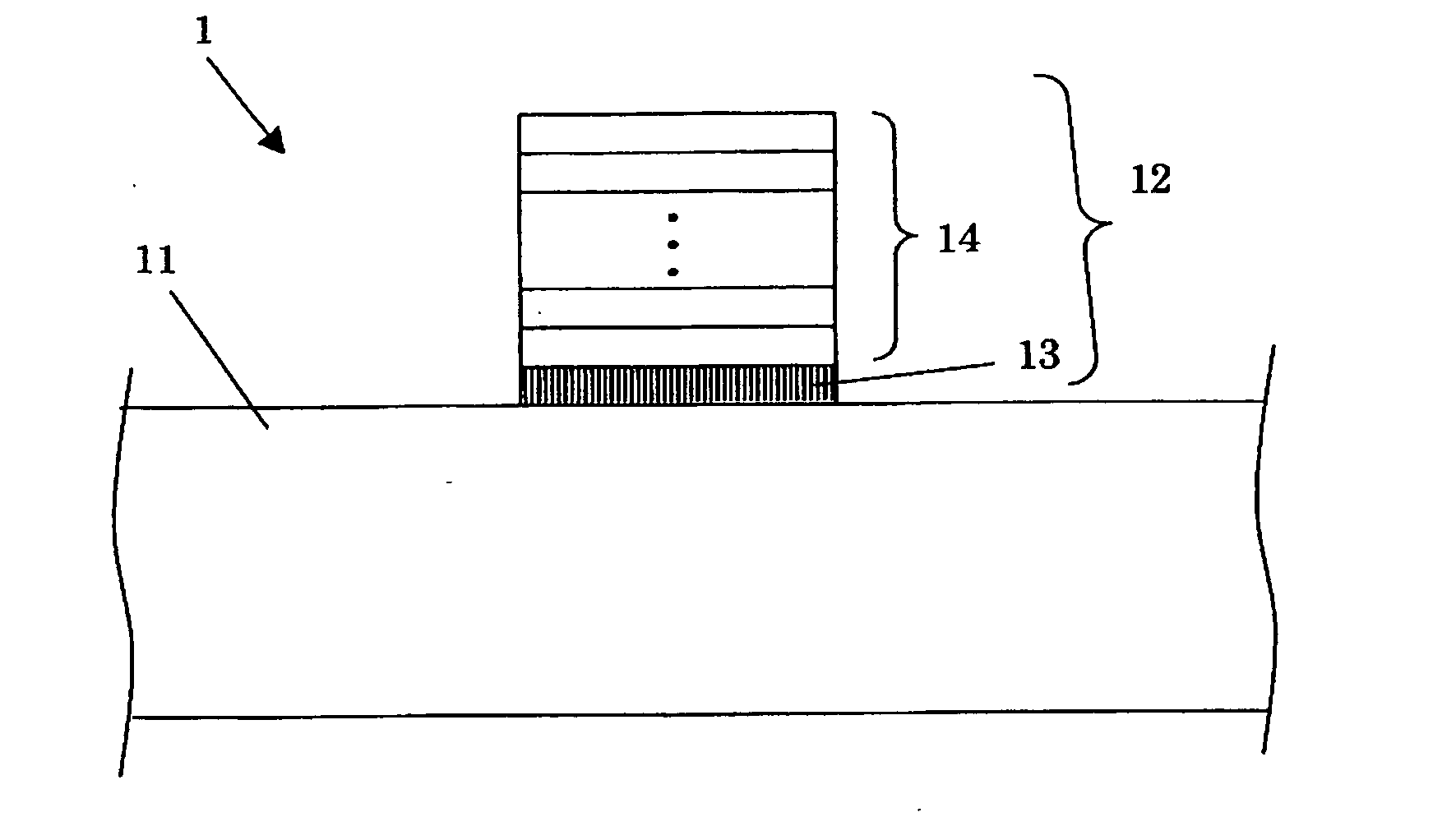
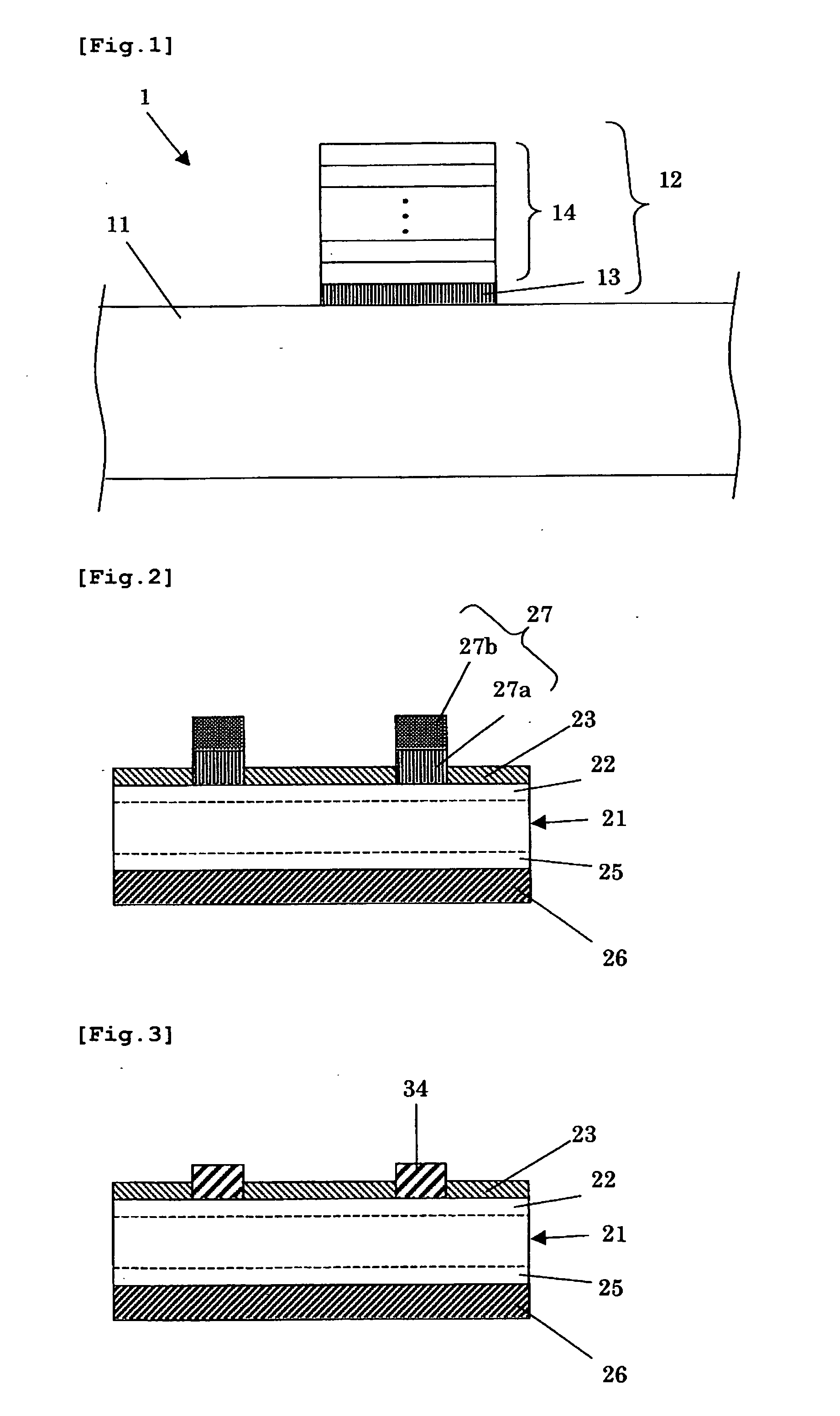
Semiconductor substrate, electrode forming method, and solar cell fabricating method
a technology of semiconductors and electrodes, applied in the direction of metal/alloy conductors, conductors, liquid/solution decomposition chemical coatings, etc., can solve the problems of degrading the characteristics of the electrode, difficult to form an electrode having a high aspect ratio, and electrode inoperative, etc., to achieve enhanced conversion efficiency, high aspect ratio, and large light receiving area
- Summary
- Abstract
- Description
- Claims
- Application Information
AI Technical Summary
Benefits of technology
Problems solved by technology
Method used
Image

Examples
examples
[0062]The present invention will be specifically described by way of Examples and Comparative Examples according to the present invention, but the present invention is not limited to those.
example 11
[0070]Ten pieces of semiconductor substrates were fabricated in the same process as in Example 1 except that there were two upper electrode layers, that is, the entire front surface electrode was constituted of three layers.
[0071]First of all, the first electrode layer was fabricated in the same manner as in Example 1. Next, the conductive pastes for the upper electrode layer mainly including the silver powder, the glass frit, the organic vehicle, and the organic solvent, in which the total silver content, the content of the silver particles having particle diameters with respect to the total silver content in the conductive paste for the upper electrode layer, the viscosity, and the thixotropy (a TI value) were shown in Table 1, were applied onto the first electrode layer, followed by drying the organic solvent in a clean oven at 150° C., thus forming the first layer in the upper electrode layer. Subsequently, the same conductive paste as that used in forming the first layer in the...
PUM
| Property | Measurement | Unit |
|---|---|---|
| particle diameter | aaaaa | aaaaa |
| particle diameter | aaaaa | aaaaa |
| particle diameter | aaaaa | aaaaa |
Abstract
Description
Claims
Application Information