Forward scattering nanoparticle enhancement method and photo detector device

Inactive Publication Date: 2009-10-08
RGT UNIV OF CALIFORNIA
View PDF1 Cites 28 Cited by
  • Summary
  • Abstract
  • Description
  • Claims
  • Application Information

AI Technical Summary

Benefits of technology

[0012]A particular preferred embodiment device is a photo detector device formed of bulk photo conversion material and having a not shallow pn junction depth. Nanoparticles are sized and arranged to forward scatter incident radiation into the photo conversion material. For silicon, a not shallow pn junction depth is at least about 0.3-0.5 μm, and preferably one to a few microns. For Group III-V materials, a not shallow junction depth is at least 100 nm and preferably a couple to a few hundred nanometers. Another preferred embodiment device is a molecular material, e.g., organic molecules or polymer, photo detector device. It is difficult to fabricate anti-reflection coatings for such materials due to their low index of refraction, but using the forward scattering of metal nanoparticles according to the invention provides an anti-reflection effect and increases photo conversion efficiency. Amorphous hydrogenated silicon devices of the invention include metal nanoparticles that are sized and arranged to forward scatter incident radiation, permitting the use of thin a-Si:H layers with increased efficiency.

Problems solved by technology

The mechanism for conversion in a typical photo detector device is often relatively inefficient.
However, there was little if any direct evidence of plasmon effects based on clear correlation of the wavelengths at which enhancement was observed with nanoparticle size and consequent plasmon wavelength.
The embedding of nanoparticles into device material layers presents fabrication issues, and can have other unintended effects.
The types of structures, materials, and thickness that can be used to incorporate metal particles and clusters is limited.
The enhancement effect consisted of the excitation of waveguided modes in the thin Si layer, resulting in greatly increased optical path length within the Si material.
This effect is not expected to be applicable to bulk semiconductor structures, in which lateral waveguiding is unlikely to occur.
2005 paper is not applicable to bulk Si photovoltaic devices, as it would require design of devices in which absorption occurs predominantly very near the device surface.
Shallow junction devices are generally not used in practical photo detector devices due to the deleterious effect of surface recombination.
Efficiency in shallow junction devices is harmed by high rates of recombination of electron and hole pairs at a semiconductor surface, which significantly reduces electrical current that is produced.
In the case of detectors, such recombination in shallow junction devices limits sensitivity.
In the case of solar cells such recombination limits power output.
In silicon devices, pn junctions are typically at least about 0.5 μm deep, with significantly smaller junction depths leading to high surface recombination, increased sheet resistance and other disadvantages for photo detector devices.
Due to cost and fabrication issues, however, silicon is the favored material system for solar cells despite its lower photo conversion efficiency compared to Group III-V material systems.
Making high purity silicon thick enough to permit addition radiation to be absorbed in the longer path-length and thereby generate sufficient energy conversion for practical use is difficult and expensive.
However, the high defect densities typically present in a-Si:H thin films limit the typical minority carrier diffusion lengths to ˜100 nm.
Limited efficiency, due mostly to insufficient material quality, and high cost of non-Si materials are the main reasons bulk Si currently dominates over all other materials for practical solar cell applications.

Method used


Image

  • Forward scattering nanoparticle enhancement method and photo detector device
  • Forward scattering nanoparticle enhancement method and photo detector device
  • Forward scattering nanoparticle enhancement method and photo detector device

Examples


Embodiment Construction

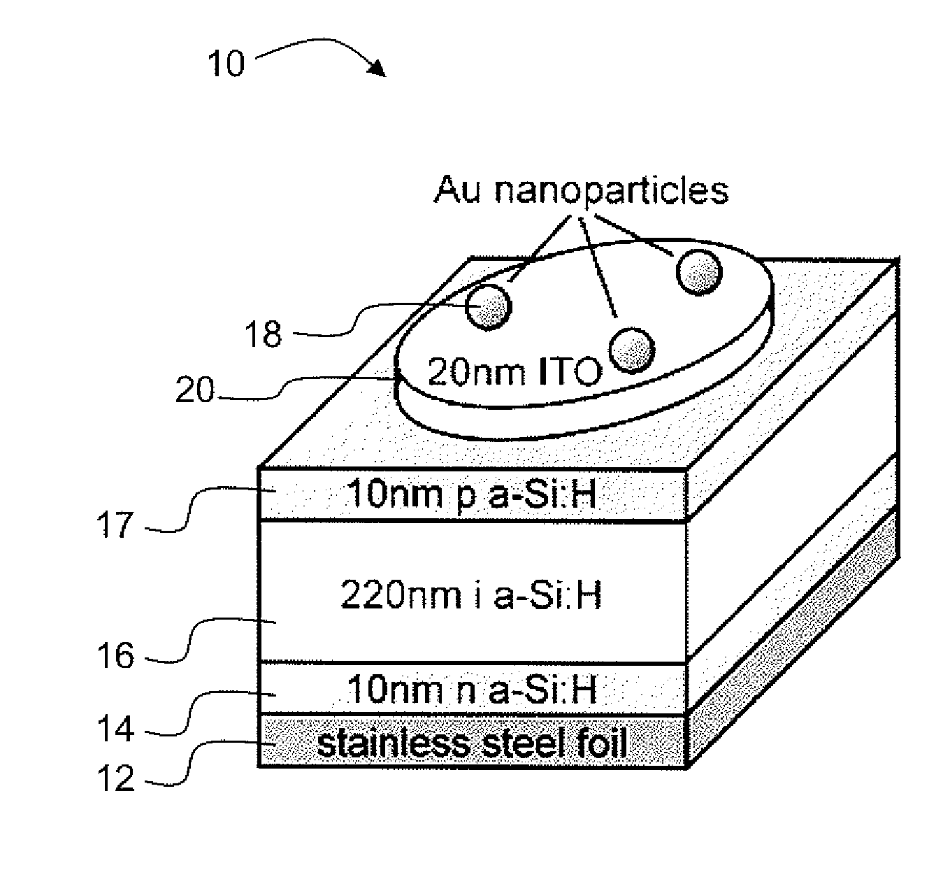
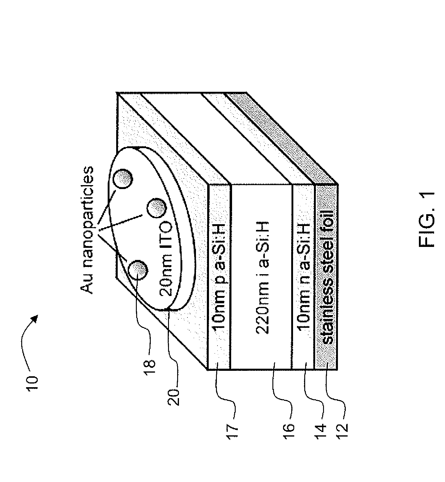
[0018]In devices of the invention, forward scattering nanoparticles are sized and arranged with respect to a photo conversion material to forward scatter radiation that would otherwise be reflected away from the photo conversion material. In preferred embodiment devices, a highest percentage of the nanoparticles are sized such that their predominant characteristic is scattering as opposed to absorption. The nanoparticles forward scatter radiation into the photo conversion material that would otherwise be reflected. In preferred embodiments, the nanoparticles are metal nanoparticles, such as gold, silver, copper, or aluminum nanoparticles, and in other embodiments the nanoparticles are dielectric nanoparticles, e.g., silica, sized to predominately forward scatter radiation.

[0019]A particular preferred embodiment device is a photo detector device formed of bulk photo conversion material and having a not shallow pn junction depth. Nanoparticles are sized and arranged to forward scatter...


PUM


Abstract

In devices of the invention, forward scattering nanoparticles are sized and arranged with respect to a photo conversion material to forward scatter radiation that would otherwise be reflected away from the photo conversion material. In preferred embodiment devices, a highest percentage of the nanoparticles are sized such that their predominant characteristic is scattering as opposed to absorption. The nanoparticles forward scatter radiation into the photo conversion material that would otherwise be reflected. In preferred embodiments, the nanoparticles are metal nanoparticles, such as gold, silver, copper, or aluminum nanoparticles, and in other embodiments the nanoparticles are dielectric nanoparticles, e.g., silica, sized to predominately forward scatter radiation.

Description

FIELD[0001]A field of the invention is energy conversion, namely radiation energy into electrical energy in photo detector devices, e.g., photovoltaic devices, solar cells, etc.BACKGROUND[0002]Photo detector devices convert electromagnetic radiation, typically at optical (far-infrared to ultraviolet) frequencies, to electrical energy. Example photo detector devices include photovoltaic devices and solar cells. Generally, an active layer absorbs photons and creates electrical current. There are many uses for photodetector devices, including applications as detectors, optical electrical communication elements, power sources, etc. The mechanism for conversion in a typical photo detector device is often relatively inefficient. There is a general recognition in the art that it would be desirable to increase the efficiency of photo detector devices. There is continued research toward that goal.[0003]Metallic nanoparticles have been embedded in the active layers of organic semiconductor ph...

Claims


Application Information

Patent Timeline
IPC IPC(8): H01L31/0264
CPCY02E10/50H01L31/02168
Inventor YU, EDWARD T.DERKACS, DANIEL
Owner RGT UNIV OF CALIFORNIA
Why Eureka
Try Eureka