Mos p-n junction schottky diode device and method for manufacturing the same

a diode and metal oxidesemiconductor technology, applied in the direction of diodes, semiconductor devices, electrical equipment, etc., can solve the problems of -n junction diodes having a forward voltage drop higher, schottky diodes have relatively low reverse voltage tolerance, and the reverse recovery time is longer, so as to achieve low forward voltage drop, improve performance, and reduce the effect of reverse leakage curren

Active Publication Date: 2009-10-22
PFC DEVICE HLDG
View PDF17 Cites 17 Cited by
  • Summary
  • Abstract
  • Description
  • Claims
  • Application Information

AI Technical Summary

Benefits of technology

[0006]The present invention provides a MOS P-N junction Schottky diode device combining a Schottky diode, an n-channel MOS structure and a P-N junction diode to achieve better performance involving low reverse leakage current, low forward voltage drop, high reverse voltage and fast reverse recovery time.
[0007]The present invention also provides a convenient and cost-effective method for manufacturing the MOS P-N junction Schottky diode device. Fewer masks are required for this manufacturing method.

Problems solved by technology

The limitations of Schottky diodes are the relatively low reverse voltage tolerance and the relatively high reverse leakage current.
The limitations are related to the Schottky barrier determined by the metal work function of the metal electrode, the band gap of the intrinsic semiconductor, the type and concentration of dopants in the semiconductor layer, and other factors.
However, the P-N junction diode has a forward voltage drop higher than that of the Schottky diode, and takes longer reverse recovery time due to a slow and random recombination of electrons and holes during the recovery period.
The TMBSR made by the aforementioned method has a low forward voltage drop but a high reverse leakage current.
Nevertheless, such device cannot resist high reverse voltage, unless the thickness of the N-type epitaxial layer 12 is increased to improve the reverse voltage tolerance.
In conclusion, Schottky diode is not suitable for high power application.
Thus, it is a challenge to design a diode device with high reverse voltage tolerance (e.g. higher than 600 V), low forward voltage drop, low reverse leakage current and fast reverse recovery time.

Method used


Image

  • Mos p-n junction schottky diode device and method for manufacturing the same
  • Mos p-n junction schottky diode device and method for manufacturing the same
  • Mos p-n junction schottky diode device and method for manufacturing the same

Examples


Embodiment Construction

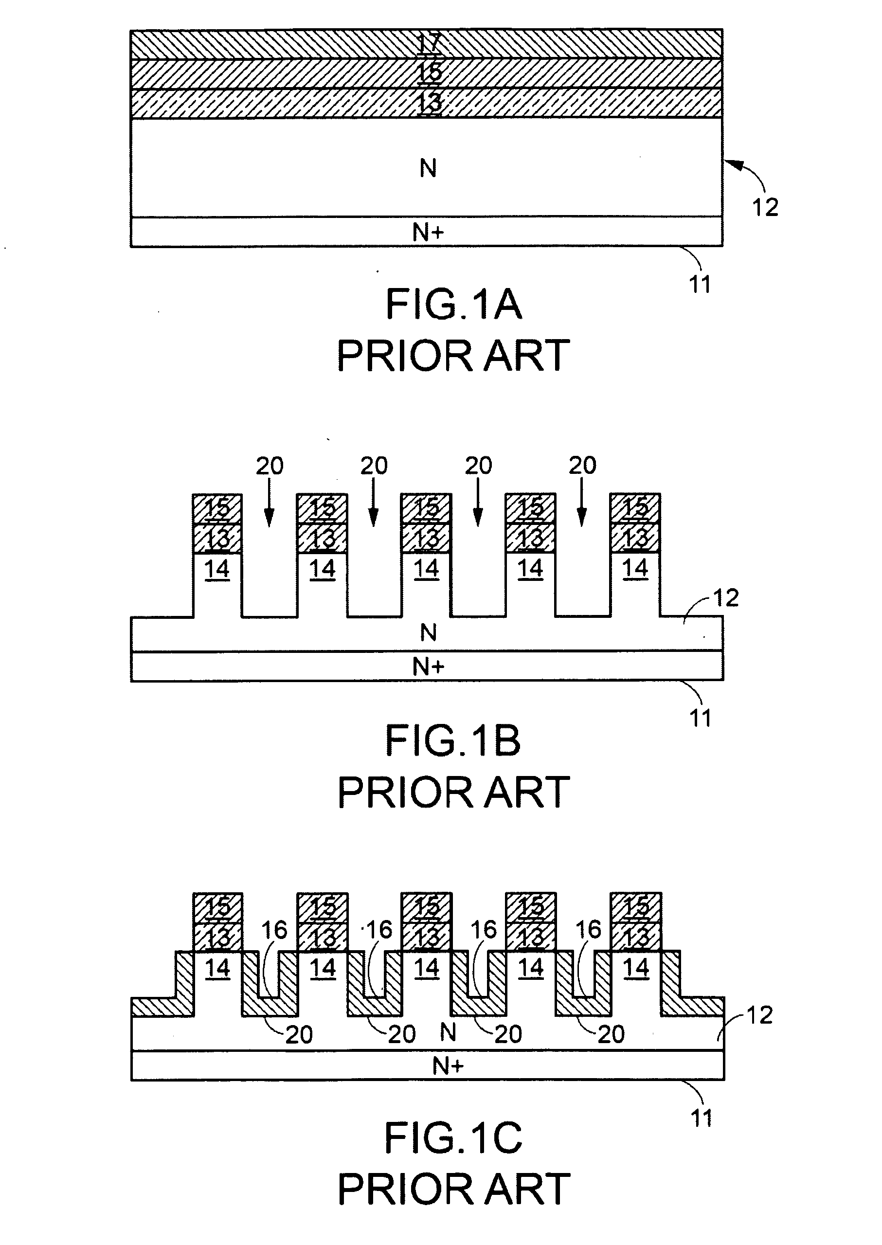
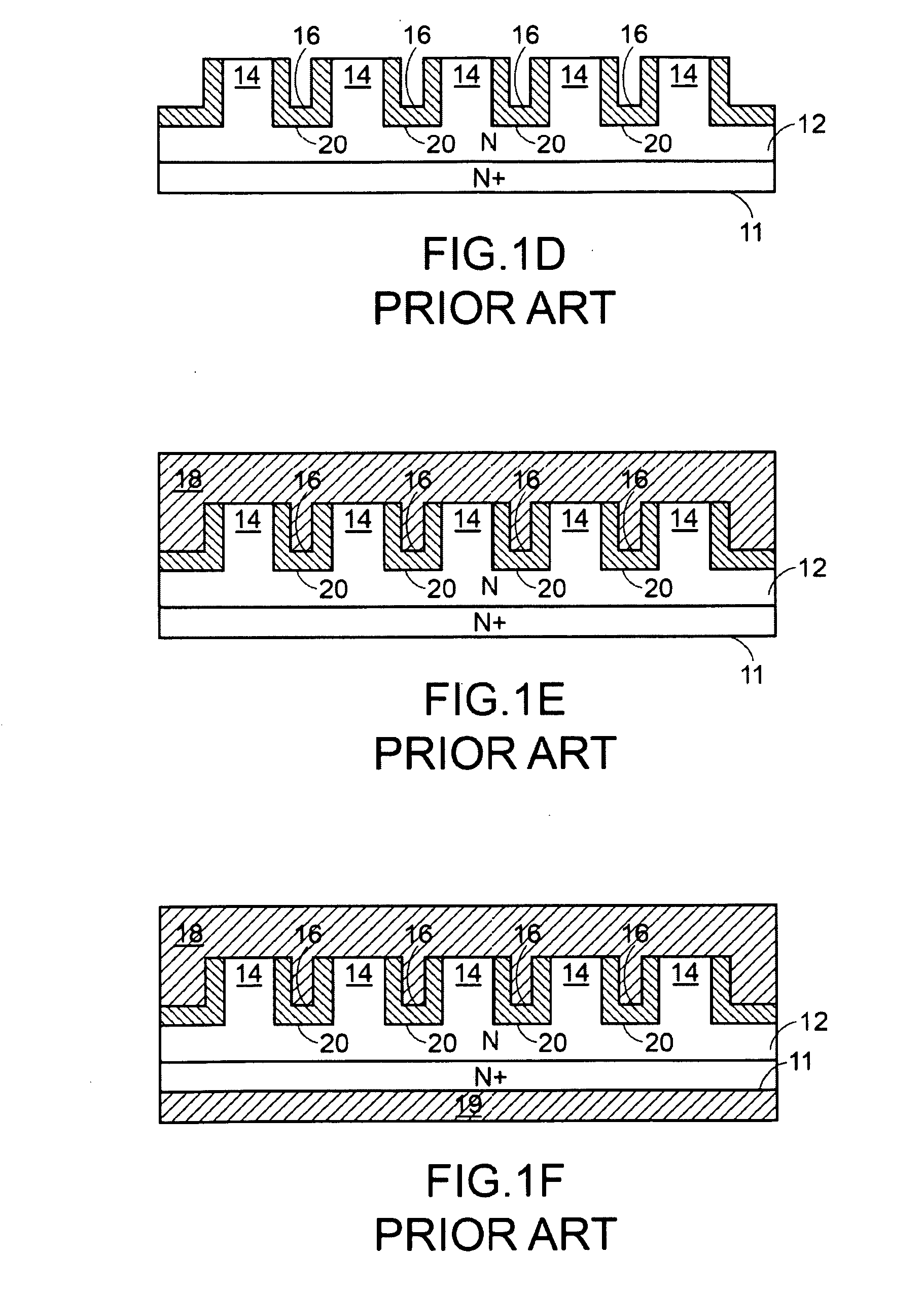
[0014]The present invention will now be described more specifically with reference to the following embodiments. It is to be noted that the following descriptions of preferred embodiments of this invention are presented herein for purpose of illustration and description only. It is not intended to be exhaustive or to be limited to the precise form disclosed.

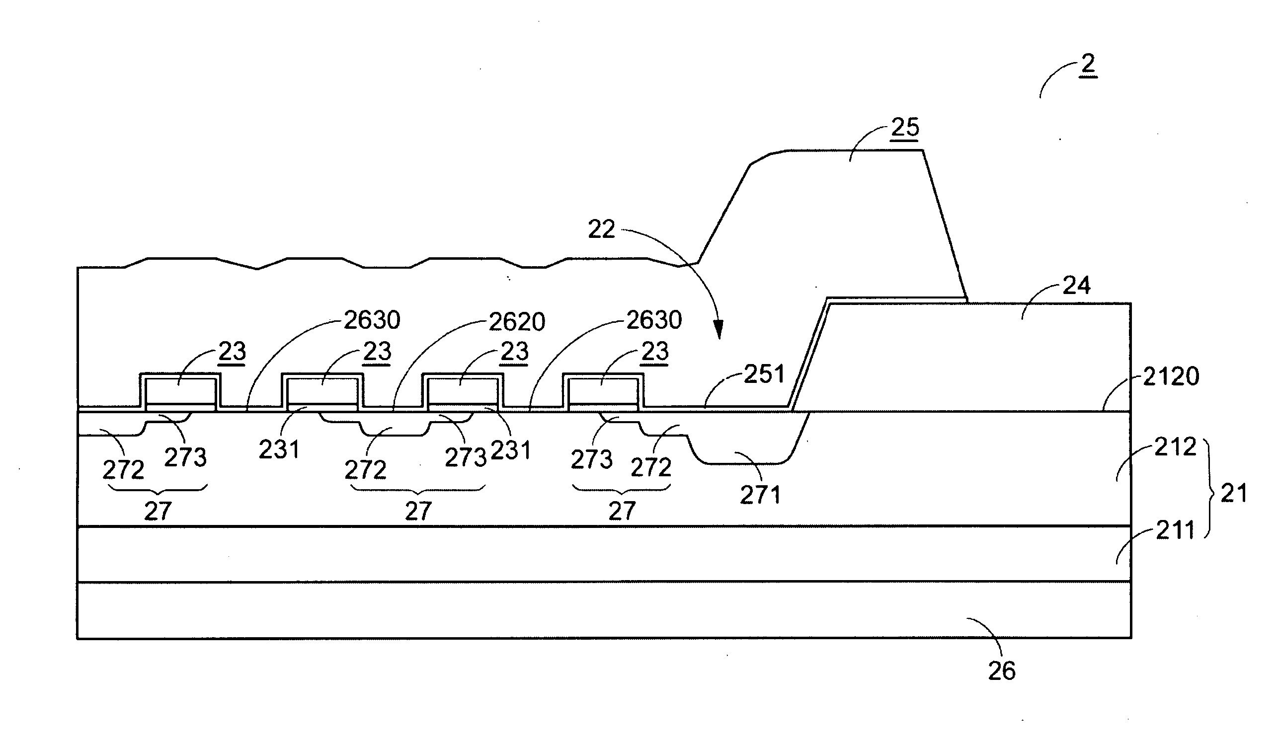
[0015]Referring to FIG. 2, FIG. 2 schematically illustrates a preferred embodiment of a MOS P-N junction Schottky diode device according to the present invention. Please note that the article “a” or “an” may be used for some elements, but the number of the elements is not limited to “one”. The amount may vary with different applications. As shown in FIG. 2, the MOS P-N junction Schottky diode device 2 primarily includes a substrate 21, a trench structure 22, a gate structure 23, a field oxide structure 24, a top electrode 25, a bottom electrode 26 and a doped region 27. The substrate 21 includes a heavily-doped N-type silicon lay...


PUM


Abstract

A MOS P-N junction Schottky diode device includes a substrate having a first conductivity type, a field oxide structure defining a trench structure, a gate structure formed in the trench structure and a doped region having a second conductivity type adjacent to the gate structure in the substrate. An ohmic contact and a Schottky contact are formed at different sides of the gate structure. The method for manufacturing such diode device includes several ion-implanting steps to form several doped sub-regions with different implantation depths to constitute the doped regions. The formed MOS P-N junction Schottky diode device has low forward voltage drop, low reverse leakage current, fast reverse recovery time and high reverse voltage tolerance.

Description

FIELD OF THE INVENTION[0001]The present invention relates to a metal-oxide-semiconductor (MOS) P-N junction Schottky diode device and a method for manufacturing the diode device, and more particularly to a MOS P-N junction Schottky diode device with low leakage current, low forward voltage drop, high reverse voltage and fast reverse recovery time.BACKGROUND OF THE INVENTION[0002]A Schottky diode is a unipolar device using electrons as carriers, which is characterized by high switching speed and low forward voltage drop. Hence, Schottky diodes are used in many applications. The limitations of Schottky diodes are the relatively low reverse voltage tolerance and the relatively high reverse leakage current. The limitations are related to the Schottky barrier determined by the metal work function of the metal electrode, the band gap of the intrinsic semiconductor, the type and concentration of dopants in the semiconductor layer, and other factors. In contrast to the Schottky diode, a P-N...

Claims


Application Information

Patent Timeline
Patent Type & Authority Applications(United States)
IPC IPC(8): H01L29/78H01L21/336
CPCH01L29/0619H01L29/0684H01L29/66143H01L29/66848H01L29/7391H01L29/872H01L29/66356
Inventor CHAO, KUO-LIANGKUO, HUNG-HSINSU, TSE-CHUAN
Owner PFC DEVICE HLDG
Why Eureka
Try Eureka