Floating gate memory device with interpoly charge trapping structure

a floating gate memory and charge trapping technology, applied in the field of nonvolatile memory devices, can solve the problems of performance degradation, performance degradation, and the technology of floating gate degrading, and achieve the effects of reducing interference between adjacent devices, constant threshold voltage, and improving data retention

Active Publication Date: 2009-10-22
MACRONIX INT CO LTD
View PDF87 Cites 223 Cited by
  • Summary
  • Abstract
  • Description
  • Claims
  • Application Information

AI Technical Summary

Benefits of technology

[0012]The present invention relates to non-volatile memory devices, and more specifically to non-volatile memory devices including a floating gate between a first tunneling barrier structure and a dielectric charge trapping structure with a second tunneling barrier structure in contact with the floating gate, in which the tunneling barriers are asymmetric. The second tunneling barrier structure can be engineered to have a different electron tunneling probability function than the first tunneling barrier structure by, for example, bandgap engineering and/or using different materials or thicknesses of materials, to encourage electrons in the floating gate to move to the dielectric charge trapping layer, while tending to prevent electron tunneling from the dielectric charge trapping layer through the floating gate to the substrate. The floating gate distributes the electric field that is affected...

Problems solved by technology

Although this technology has been widely successful, as the sizes of the memory cells and the distances between them shrink, the floating gate technology starts to degrade because of interference between neighboring floating gates.
It is found that even SONOS-type memory cells can suffer performance degradation as the minimum feature size goes below about 45 nanometers.
In particula...

Method used


Image

  • Floating gate memory device with interpoly charge trapping structure
  • Floating gate memory device with interpoly charge trapping structure
  • Floating gate memory device with interpoly charge trapping structure

Examples


Embodiment Construction

[0060]A detailed description is provided with reference to FIGS. 1-28.

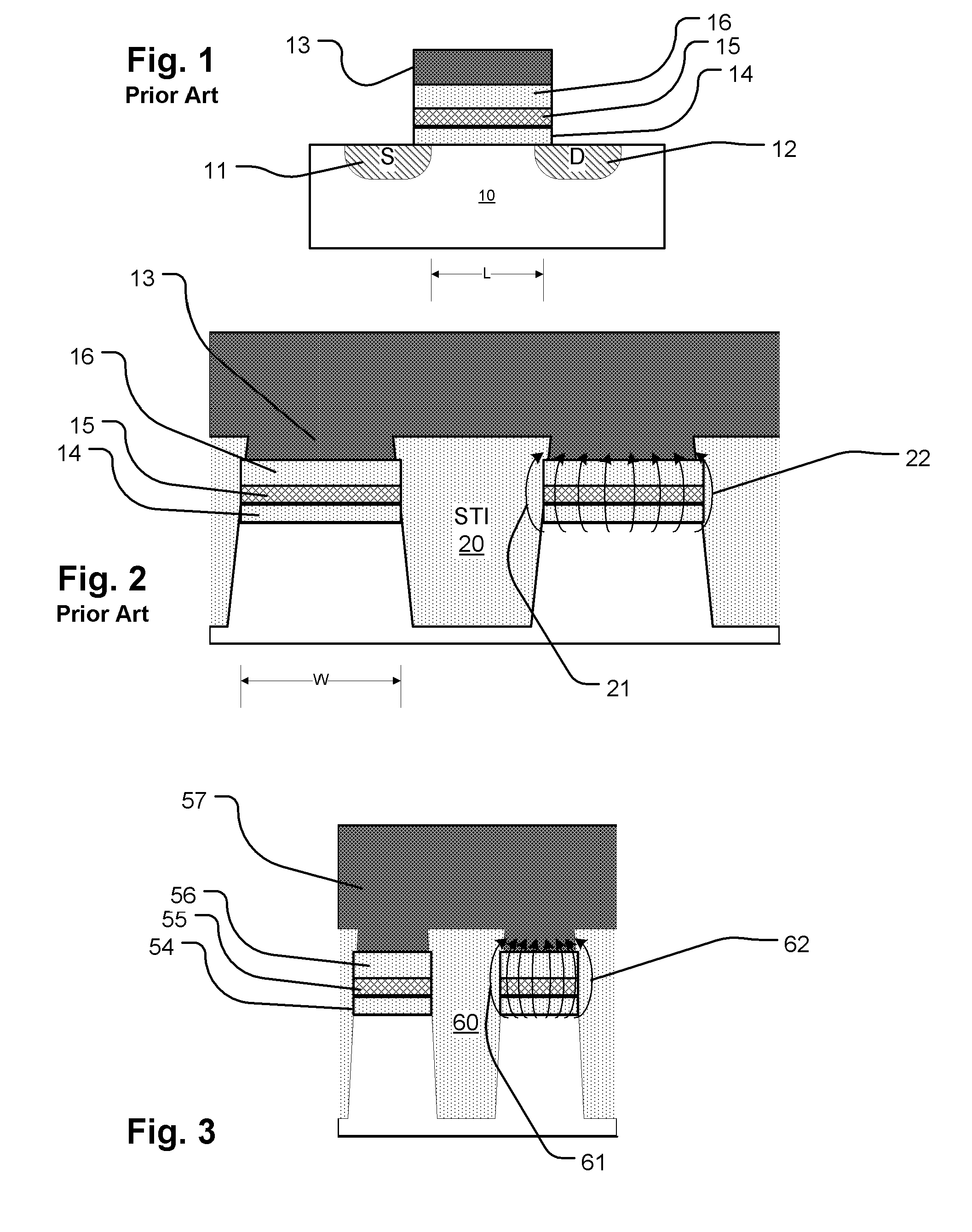
[0061]FIG. 1 illustrates the basic structure of a prior art SONOS-type memory cell. The cell is formed on a semiconductor substrate 10 in which a first doped region 11 acts as a source terminal and a second doped region 12 acts as a drain terminal. A control gate 13 is formed over a charge trapping structure which includes a bottom tunneling barrier structure 14, a dielectric charge trapping layer 15, and a top dielectric 16. The channel of the memory cell is the region of the substrate 10 between the first doped region 11 and the second doped region 12. The dimension L shown in FIG. 1 is typically referred to as the channel length L, because current flows between the source and drain along this dimension of the channel. The SONOS-type memory cell shown in FIG. 1 is often configured in a NAND array configuration, in which a column in the array includes sets of memory cells arranged in series between a ground conta...


PUM


Abstract

A charge trapping floating gate is described with asymmetric tunneling barriers. The memory cell includes a source region and a drain region separated by a channel region. A first tunneling barrier structure is disposed above the channel region. A floating gate is disposed above the first tunneling barrier structure covering the channel region. A second tunneling barrier is disposed above the floating gate. A dielectric charge trapping structure disposed above the second tunneling barrier and a blocking dielectric structure is disposed above the charge trapping structure. A top conductive layer disposed above the top dielectric structure acts as a gate. The second tunneling barrier is a more efficient conductor of tunneling current, under bias conditions applied for programming and erasing the memory cell, than the first tunneling barrier structure.

Description

RELATED APPLICATIONS[0001]This application claims the benefit of U.S. Provisional Application Ser. No. 61 / 124,652 filed 18 Apr. 2008.[0002]The present application is related to co-pending U.S. patent application Ser. No. 11 / 756,559, filed 31 May 2007, entitled CHARGE TRAPPING DEVICES WITH FIELD DISTRIBUTION LAYER OVER TUNNELING BARRIER, which is incorporated by reference as if fully set forth herein.BACKGROUND OF THE INVENTION[0003]1. Field of the Invention[0004]The invention relates generally to non-volatile memory devices, and in particular to flash memory and manufacturing of flash memory devices.[0005]2. Description of Related Art[0006]Flash memory technology includes memory cells that store charge between the channel and gate of a field effect transistor. The charge stored affects the threshold of the transistor, and the changes in threshold due to the stored charge can be sensed to indicate data.[0007]One type of charge storage memory cell in widespread application is known as...

Claims


Application Information

Patent Timeline
IPC IPC(8): G11C16/06H01L29/788H01L29/792H01L21/336
CPCG11C16/0408G11C16/10H01L21/28273H01L21/28282H01L27/115H01L27/11521H01L29/792H01L27/11568H01L27/11573H01L29/42324H01L29/4234H01L29/7883H01L27/11526H01L29/40114H01L29/40117H10B41/40H10B43/40H10B43/30H10B69/00H10B41/30H01L29/66833
Inventor LUE, HANG-TING
Owner MACRONIX INT CO LTD
Why Eureka
Try Eureka