Method for growing carbon nanotubes, and electronic device having structure of ohmic connection to carbon element cylindrical structure body and production method thereof

Active Publication Date: 2009-10-29
FUJITSU LTD
View PDF4 Cites 5 Cited by
  • Summary
  • Abstract
  • Description
  • Claims
  • Application Information

AI Technical Summary

Benefits of technology

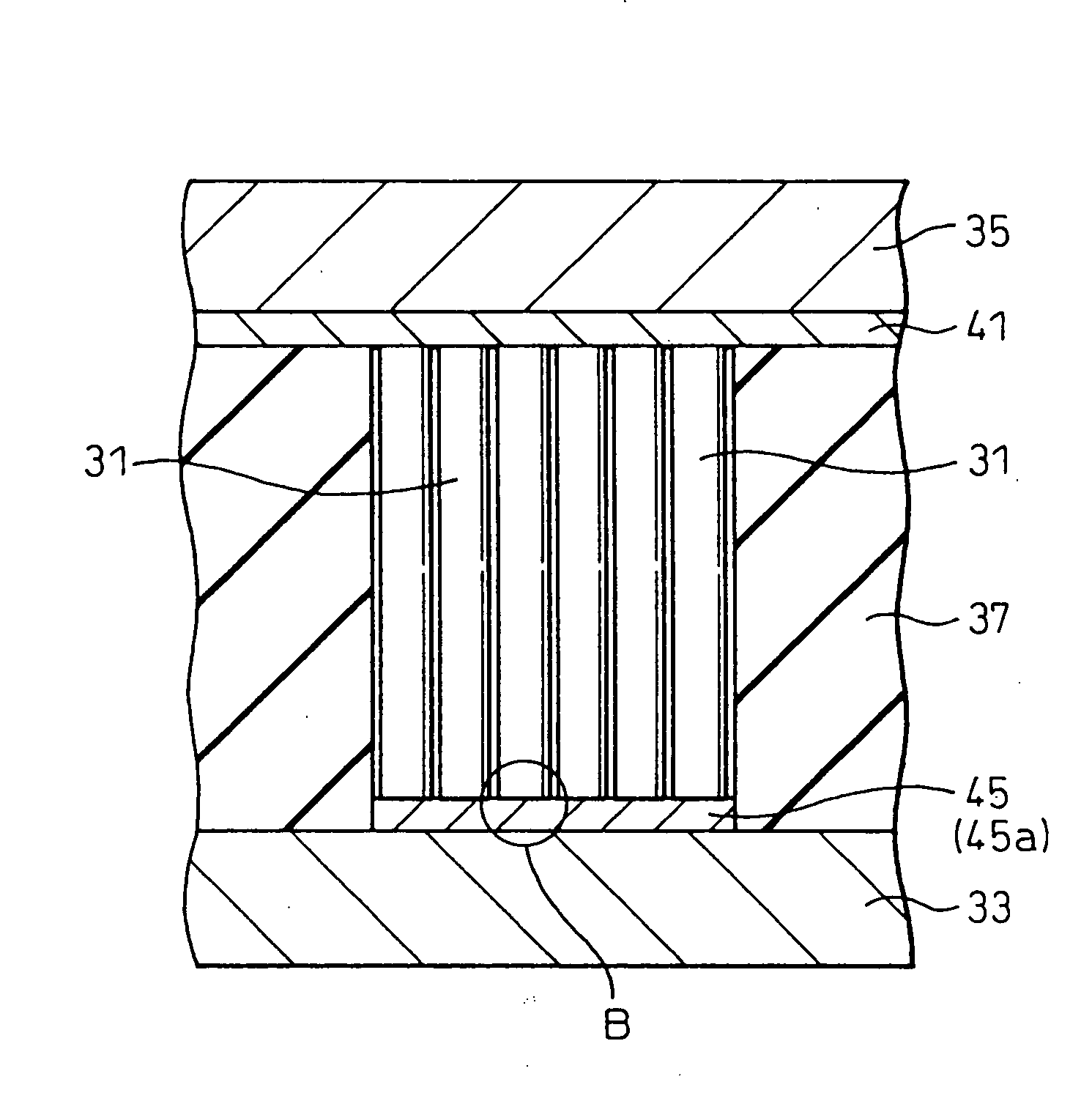
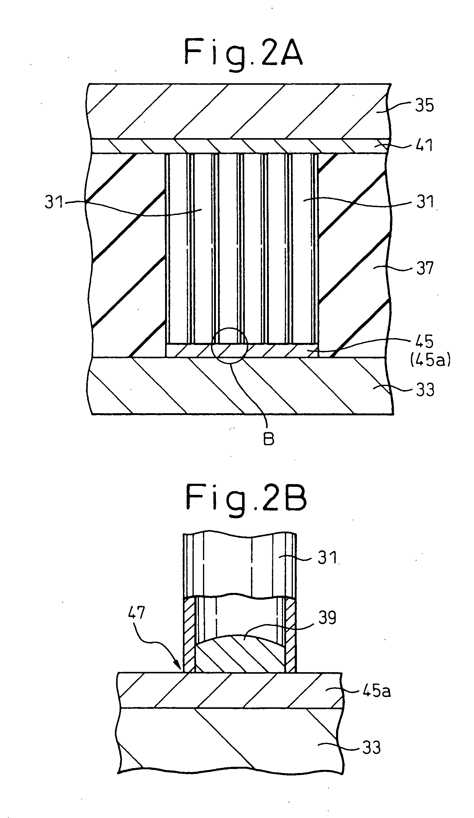
[0017]The electronic device having a structure of an ohmic connection to a carbon element cylindrical structure body according to the present invention is characterized in that a metal material is positioned inside the junction part of a carbon element cylindrical structure body joined to a connection objective and the carbon element cylindrical structure body and the connection objective are connected by an ohmic contact. By virtue of connection through an ohmic contact, the increase in resistance at the connected part between the carbon element cylindrical structure body and the connection objective can be suppressed.

Problems solved by technology

By the arc discharge or laser evaporation method, a carbon nanotube having good quality can be obtained but the orientation or length of carbon nanotubes can hardly be controlled.
495-496 (2002), however, the growth temperature is as high as 800° C. or more and therefore, it is impossible to grow carbon nanotubes on a semiconductor circuit by this technique.
2229-234 (2002), however, the growth direction cannot be controlled.

Method used


Image

  • Method for growing carbon nanotubes, and electronic device having structure of ohmic connection to carbon element cylindrical structure body and production method thereof
  • Method for growing carbon nanotubes, and electronic device having structure of ohmic connection to carbon element cylindrical structure body and production method thereof
  • Method for growing carbon nanotubes, and electronic device having structure of ohmic connection to carbon element cylindrical structure body and production method thereof

Examples


example 1

[0065]In this Example, a case where the present invention is applied to an electronic device having a wiring via is described.

[0066]As shown in FIG. 5A, an SiO2 interlayer insulating film 103 (500 nm) is deposited on a lower wiring Cu layer 101 on a substrate (not shown) and thereon, a resist pattern (not shown) having openings, in the regions at which wiring vias are to be formed, is formed. By using the resist pattern as the mask, a wiring via 105 is formed in the interlayer insulating film 103. Thereafter, a Ti layer (50 nm) and an Ni catalyst metal layer (10 nm) are deposited in this order on the entire surface of the substrate by sputtering or evaporation. Subsequently, a Ti layer 107 (50 nm) / Ni layer 109 (10 nm) laminate film is caused to remain in the wiring via by the lift-off method using the resist film. In place of the Ni layer, a layer formed of Fe or Co may be used as the catalyst metal layer or a layer of an alloy containing at least one of Ni, Fe and Co may also be us...

example 2

[0070]In this Example, a case where the present invention is applied to an electronic device having a transverse wiring is described.

[0071]As shown in FIG. 6A, an SiO2 insulating film 123 (500 nm) is deposited on an Si substrate 121 and thereon, a resist pattern (not shown) having openings in the regions, at which electrodes are to be formed, is formed. On the entire surface of the substrate, a Ti layer (50 nm) and an Ni catalyst metal layer (10 nm) are deposited in this order by sputtering or evaporation.

[0072]Subsequently, only a Ti layer 125 (50 nm) / Ni layer 127 (10 nm) laminate film (electrode pattern) in the openings of the resist pattern is caused to remain by the lift-off method using the resist film.

[0073]Between a pair of opposing electrode patterns, a carbon nanotube 129 is grown by CVD (see, FIG. 6B). The CVD and growth conditions used may be the same as those described in Example 1. Also, similarly to Example 1, the Ni / Ti laminate film may be heat-treated in advance of t...

example 3

[0074]As shown in FIG. 8A, an Ni thin film 222 for catalyst was formed on a silicon substrate 220 by evaporation and, thereon, an SiN insulating film 224 (thickness: 500 nm) having an opening with a diameter of 2 μm was formed. The thickness of the Ni thin film 222 can be arbitrarily decided, but the thickness was set here to 2 nm. This substrate was introduced into a reaction part (vacuum chamber) (not shown) and the substrate temperature was set to 500° C. A starting material gas prepared by mixing argon and acetylene at a ratio of 80:20 was supplied to the reaction part at a flow rate of 100 ccm and the total gas pressure in the reaction part was adjusted to 1 kPa by the control in an exhaust system connected to a vacuum pump. A hot filament (made of rhenium) was moved above the substrate and with a distance of about 6 mm to the substrate, a current of about 8 A was passed. By this passing of a current, the hot filament temperature was elevated to 800° C. After maintaining this s...


PUM

PropertyMeasurementUnit
Temperatureaaaaaaaaaa
Structureaaaaaaaaaa
Electric fieldaaaaaaaaaa

Abstract

An electronic device having a structure of an ohmic connection to a carbon element cylindrical structure body, wherein a metal material is positioned inside the junction part of a carbon element cylindrical structure body joined to a connection objective and the carbon element cylindrical structure body and the connection objective are connected by an ohmic contact. Methods for producing such an electronic device are also disclosed. Further, a method for growing a carbon nanotube is disclosed.

Description

CROSS-REFERENCES TO RELATED APPLICATIONS[0001]This application is based upon and claims the benefit of priority from each of prior Japanese Patent Applications No. 2003-078353, filed on Mar. 20, 2003, and No. 2003-083192, filed on Mar. 25, 2003, the entire contents thereof being incorporated herein by reference.BACKGROUND OF THE INVENTION[0002]1. Field of the Invention[0003]The present invention relates to an electronic device having a structure for ohmic connection to a carbon element cylindrical structure body represented by a carbon nanotube and a production method thereof, which techniques are widely applicable when a carbon element cylindrical structure body is applied to an electronic device.[0004]The present invention also relates to a method for growing carbon nanotubes.[0005]2. Description of the Related Art[0006]In recent years, studies are being made on the use of a carbon element cylindrical structure body as an electrically conducting or semiconductor material in an ele...

Claims


Application Information

Patent Timeline
IPC IPC(8): H01L21/285C23C16/26H01L21/768H05K3/40
CPCB82Y10/00B82Y30/00C23C16/26H05K3/4076H01L21/76838H01L21/76879H01L2221/1094H01L21/28562
Inventor KAWABATA, AKIONIHEI, MIZUHISA
Owner FUJITSU LTD
Why Eureka
Try Eureka