

Vacuum Electronic Devices and Cavities and Fabrication Methods Therefor
a technology of vacuum electronic devices and cavities, applied in the direction of discharge tubes/lamp details, amplifiers with transit-time effect, discharge tubes luminescnet screens, etc., can solve the problems of high-order multipliers that are inefficient, require millions of dollars of investment, and are very expensiv
- Summary
- Abstract
- Description
- Claims
- Application Information
AI Technical Summary
Benefits of technology
Problems solved by technology
Method used
Image

Examples
examples
[0082]In accordance with certain embodiments of the invention, exemplary devices were prepared and evaluated.
example a
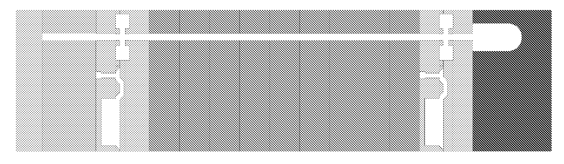
See FIGS. 36a-e
[0083]A THz emitter array Klystron was fabricated, as generally illustrated in FIGS. 36a-e. The fabrication methods utilized DRIE etching and wafer-level (or die-level) fusion bonding of silicon wafers to form a negative mold that was coated with sputtered or electrodeposited copper. In one embodiment, ‘stock’ FEA was fusion-bonded to the base of the tube stack, with beam diameter confined by a magnetic field aligned with the axis of the tube. The fabrication process provided excellent alignment of the magnetic field with the tube axis, and allowed for easy integration of the electron gun.
[0084]Certain benefits of the fabricated klystron include: better power density and efficiency compared to solid-state or other VED alternatives; continuous-wave THz and / or mm-wave band source; and a three-phase program that will produce a klystron array integrated into a prototype system.
[0085]Power Density (limited by ability to cool): 25 MW / m3
[0086]Efficiency 1% or better
example b
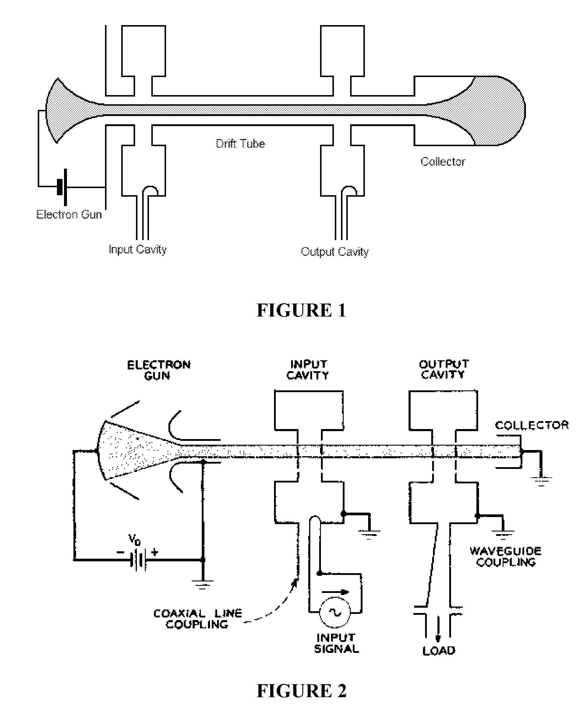
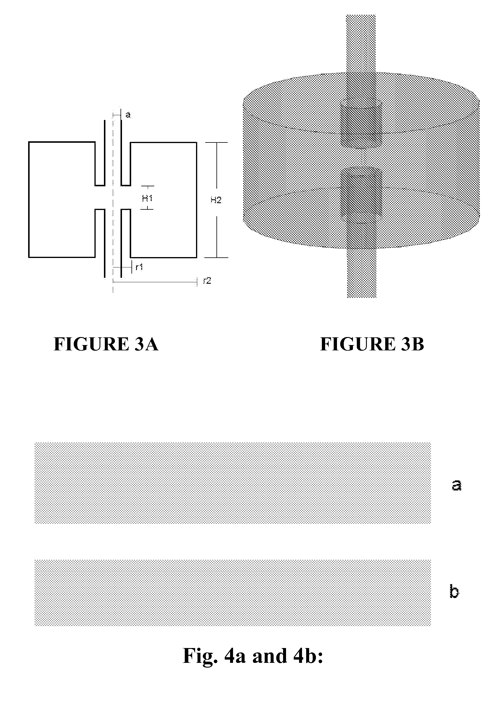
[0087]A 2-cavity kylstron was prepared according to fabrication methods of the invention. The beam tunnel diameter for both current, and cavity coupling was optimized while making some reasonable assumptions about current density and filling factor results in a beam tunnel radius of 35 μm, and a beam radius of 25 μm. To obtain such a fine beam with a conventional thermionic cathode would require beam shaving, which would significantly lower the tube efficiency. The alternate approach is to use a FEA, which can produce the necessary current density without beam compression. This also allows for easy integration with a micro-fabricated tube, and simplifies the magnetic field design.
[0088]FEAs are capable of producing very high current densities, often exceeding several hundred A / cm2 in ideal conditions. A vacuum tube environment provides less than ideal conditions for an FEA, however it does seem reasonable to expect current densities up to 40 A / cm2. Additionally, FEA performance impr...
PUM
 Abstract
Description
Claims
Application Information