Electromagnetic wave resonator, method of manufacturing the same, and method of resonating eletromagnetic wave

a technology of eletromagnetic wave and plasmon resonance, which is applied in the field of electromagnetic wave resonators, can solve the problems of insufficient reproducibility and reliability, the gap size is limited to several tens of nanometers, and the plasmon resonance in the nanoparticle system cannot be easily used as a resonator, etc., to achieve excellent reproducibility and efficiency, and maximize electromagnetic energy

Inactive Publication Date: 2009-12-03
NAT INST FOR MATERIALS SCI
View PDF3 Cites 16 Cited by
  • Summary
  • Abstract
  • Description
  • Claims
  • Application Information

AI Technical Summary

Benefits of technology

[0016]Another aspect of the present invention provides an electromagnetic wave resonator, including a first negative dielectric surface, a second negative dielectric surface and a positive dielectric thin film disposed between the first and the second negative dielectric surfaces. The positive dielectric thin film has an end face having an electromagnetic wave introduced therefrom. A length L, the length L being a length in a principal direction of propagation of the electromagnetic wave in a region having the positive dielectric thin film sandwiched between the first and the second negative dielectric surfaces, is set such that the absolute value of a difference (L−L0) between the length L and a length L0 falls within a range of 50% or less of the length L0, the length L0 being a length in the principal direction of propagation and the length L0 maximizing electromagnetic energy which is stored in and around the positive dielectric thin film by a surface wave, the surface wave being generated by incidence of an electromagnetic wave with a predetermined wavelength from the end face, having an electric field component in a direction of film thickness of the positive dielectric thin film, and without having a cut-off frequency.
[0017]Still another aspect of the present invention provides a method of resonating an electromagnetic wave having a pre...

Problems solved by technology

Such resonance is, however, incidentally formed by random aggregation of the particles, and the reproducibility and the reliability are insufficient.
Accordingly, the plasmon resonance in the nanoparticle system cannot be used easily as a resonator.
Surface plasmons in periodic nano apertures are, however, under theoretical review, and how to achieve an extremely narrow (for example, a...

Method used


Image

  • Electromagnetic wave resonator, method of manufacturing the same, and method of resonating eletromagnetic wave
  • Electromagnetic wave resonator, method of manufacturing the same, and method of resonating eletromagnetic wave
  • Electromagnetic wave resonator, method of manufacturing the same, and method of resonating eletromagnetic wave

Examples


first example

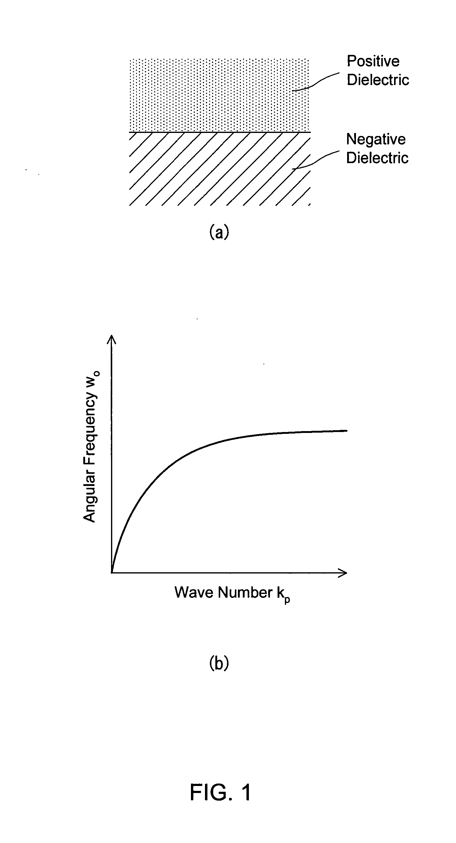
[0076]First Example illustrates an open resonator, in which gold is employed for a dielectric and surface plasmon is used as a surface wave, for an electromagnetic wave in the regions from visible light to infrared light.

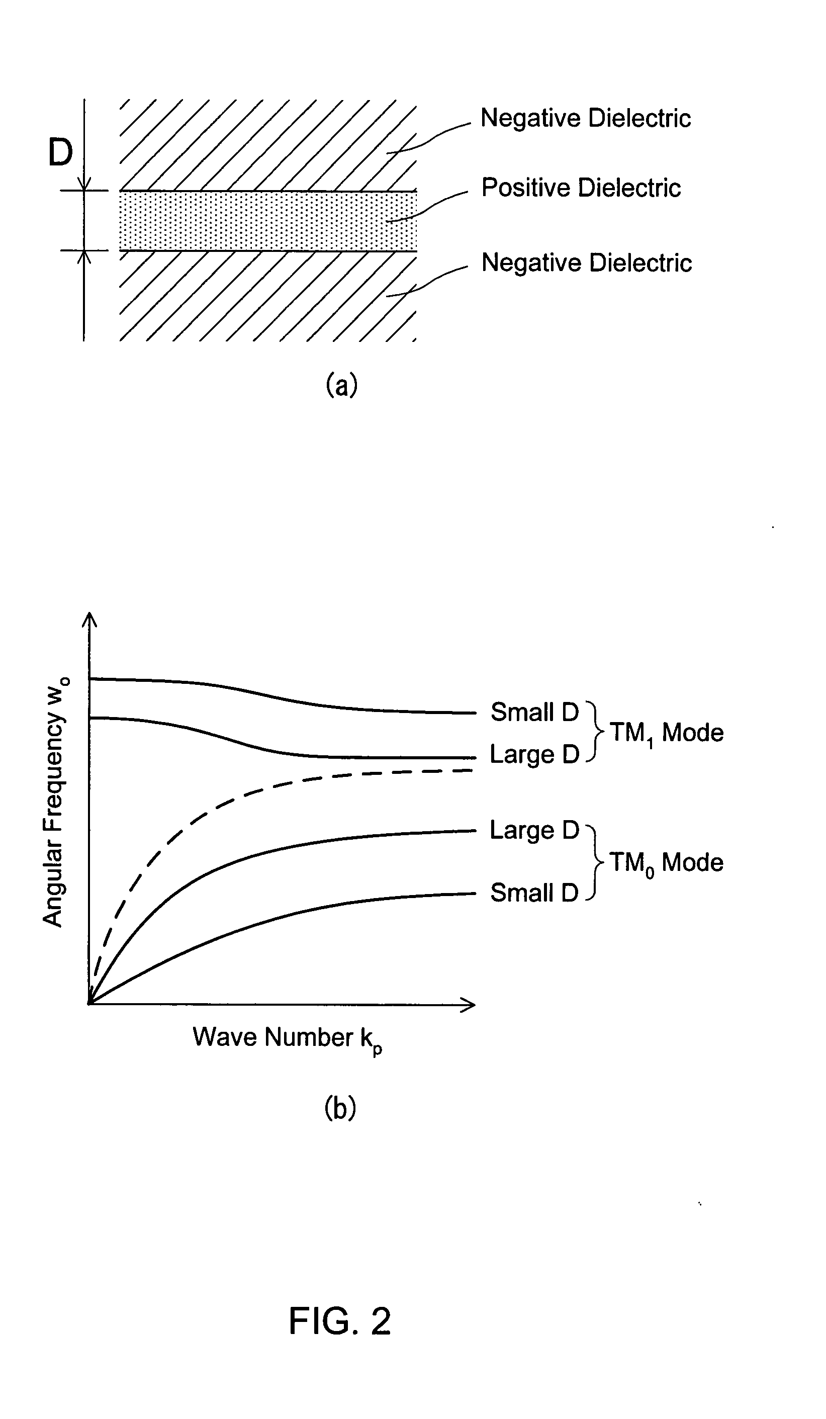
[0077]First, as shown in FIG. 6(a), a first negative dielectric thin film 1, a positive dielectric thin film 3, and a second negative dielectric thin film 2 were formed on a substrate 10 in this order. In this Example, a synthetic quartz substrate was employed for the substrate 10. On this substrate, a gold thin film with a thickness of 150 nm as the first negative dielectric thin film 1, a silica (SiO2) thin film with a thickness D as the positive dielectric thin film 3 and a gold thin film with a thickness of 150 nm as the second negative dielectric thin film 2 were stacked.

[0078]The gold thin films were formed by DC magnetron sputtering and the silica thin film was formed by high frequency magnetron sputtering. A chromium film with a thickness in a range from 5 n...

second example

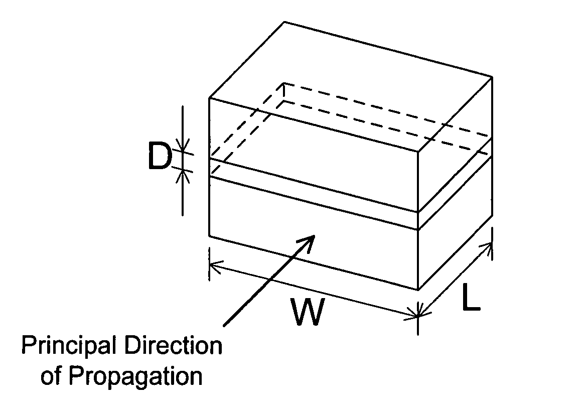
[0098]The second Example was to realize a closed resonator under the conditions almost same as the first Example. The same procedure as the first Example was carried out until forming a stacked film of a first negative dielectric thin film (a gold thin film) 1, a positive dielectric thin film (a silica thin film) 3 and a second negative dielectric thin film (gold) 2 on a substrate (a synthetic quartz substrate) 10 and removing the outside by focused ion beam so as to leave the rectangular resonator with a length L′ and a width W′ (FIG. 9(a)). The length L′ and the width W′ should be defined rather large in size, such as 500 nm. The depth for removal should be at least so deep as to pass through the second negative dielectric thin film 2.

[0099]The substrate was moved into a resistive heating vacuum evaporator to deposit a gold thin film with a thickness of 150 nm as a third negative dielectric thin film 4 (FIG. 9(b)). In this process, the substrate was positioned to be 45 degrees obl...

third example

[0103]In the third Example, a resonator is described that has a plurality of the resonance structures as described in the first and the second Examples aligned therein. It is important for practical use to realize a resonator aligned to interact with electromagnetic waves emitted to a wide region.

[0104]A method of manufacturing a resonator having a plurality of open resonator structures aligned therein is illustrated here. First, a multilayer (a multilayer structure) 11 is formed in which a gold thin film with a thickness of 150 nm as a negative dielectric thin film 7 and a silica thin film with a thickness D as a positive dielectric thin film 3 were stack with each other a plurality of times on a synthetic quartz substrate as a substrate 10 (FIG. 10(a)).

[0105]Subsequently, the substrate 10 was cut into strips each with a width of, for example, 2 mm. One of the strips was paired with another and the multilayer structure parts were bonded with a hard epoxy resin to be a junction laye...


PUM

PropertyMeasurementUnit
Lengthaaaaaaaaaa
Thicknessaaaaaaaaaa
Thicknessaaaaaaaaaa

Abstract

The present invention provides an electromagnetic wave resonator that is capable of showing surface wave resonance typically as outstanding plasmon resonance and can be manufactured industrially with excellent reproducibility and efficiency by combining currently available microprocessing technologies. The electromagnetic wave resonator of the present invention includes a first negative dielectric surface, a second negative dielectric surface and a positive dielectric thin film disposed between the first and the second negative dielectric surfaces. The positive dielectric thin film has an end face having an electromagnetic wave introduced therefrom. Intensity of the electromagnetic wave having a predetermined wavelength and being introduced from the end face is enhanced in the electromagnetic wave resonator due to resonance of a surface wave having an electric field component in a direction of film thickness of the positive dielectric thin film and without having a cut-off frequency.

Description

TECHNICAL FIELD[0001]The present invention relates to an electromagnetic wave resonator used for enhancing an electromagnetic field in a frequency range including microwaves, millimeter waves, terahertz waves, infrared rays, visible rays and ultraviolet rays, the resonator having dimensions about the same as or more minute than the wavelength.BACKGROUND ART[0002]Electromagnetic wave resonators are essential for generating and amplifying of coherent electromagnetic waves, wavelength selection, highly sensitive detection of an electromagnetic wave due to enhancement of an electromagnetic field, and exhibiting various non-linear effects.[0003]With respect to light such as infrared rays, visible rays and ultraviolet rays, conventional resonators are composed of geometric optical elements and have much larger volumes than those of the wavelengths. A typical example of them is a laser oscillator composed of dielectric multilayer mirrors. In recent years, however, researches and developmen...

Claims


Application Information

Patent Timeline
IPC IPC(8): H01P7/10H01P11/00
CPCB82Y20/00Y10T29/49016G02B6/1226
Inventor MIYAZAKI, HIDEKIKUROKAWA, YOICHI
Owner NAT INST FOR MATERIALS SCI
Why Eureka
Try Eureka