

Apparatus and method for improving production throughput in CVD chamber
a technology of apparatus and chamber, which is applied in the field of apparatus and methods for improving the production throughput of cvd chamber, can solve the problems of insufficient cleaning at the locations, time-consuming processes of known remote plasma cleaning techniques, and short oxygen ions, so as to reduce the frequency of cleaning and prolong the length of cleaning cycle. , the effect of reducing the frequency of cleaning
- Summary
- Abstract
- Description
- Claims
- Application Information
AI Technical Summary
Benefits of technology
Problems solved by technology
Method used
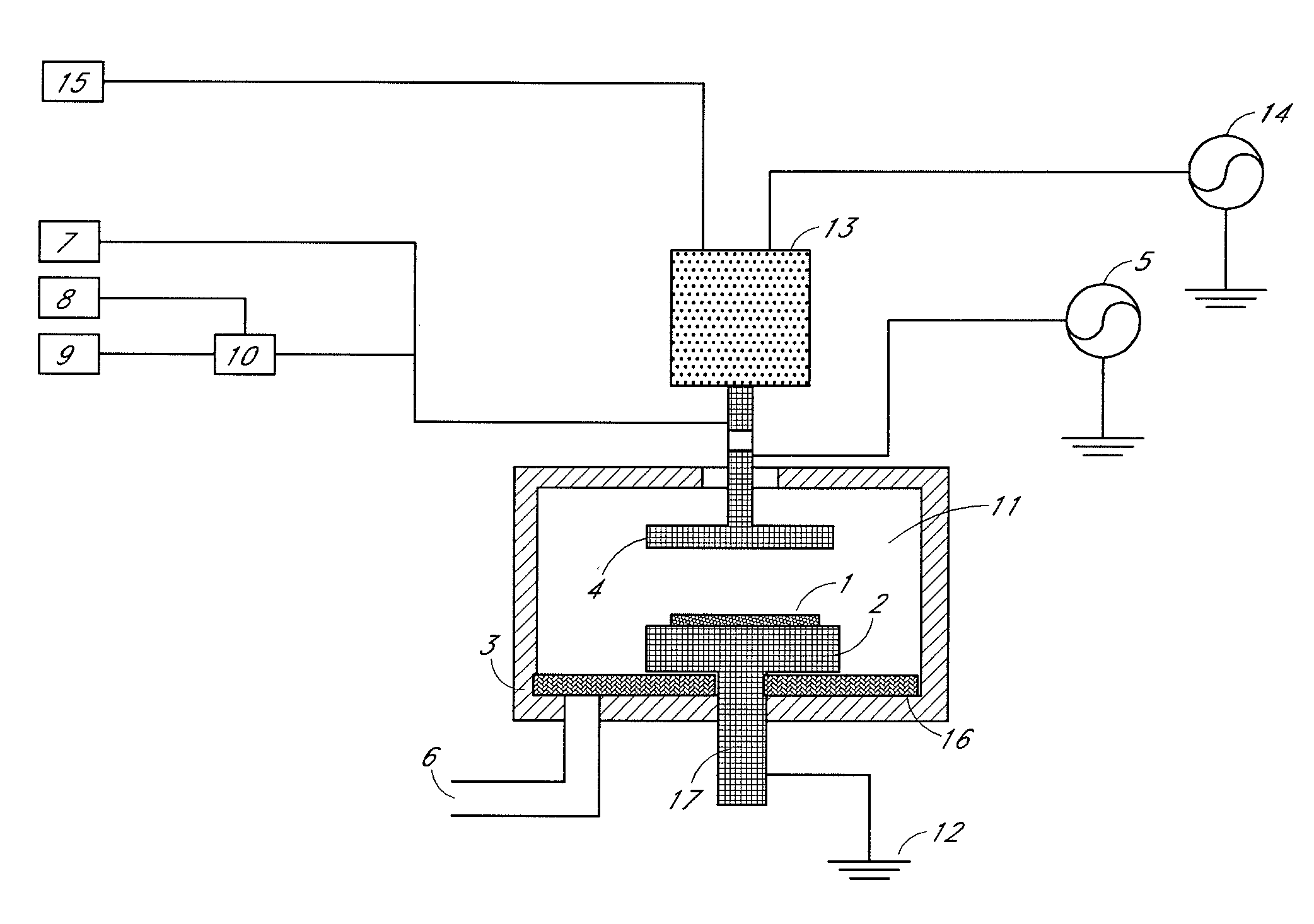
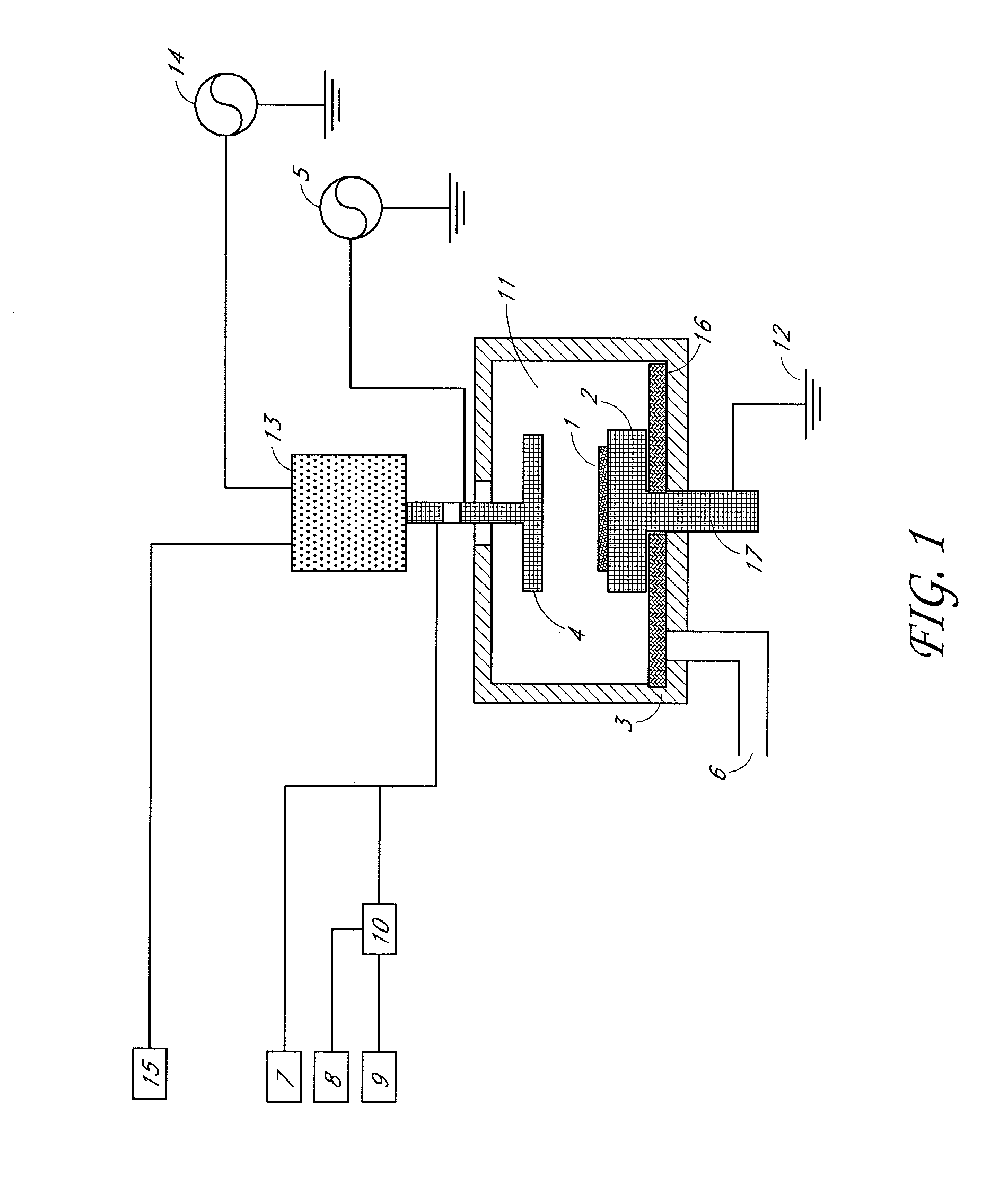
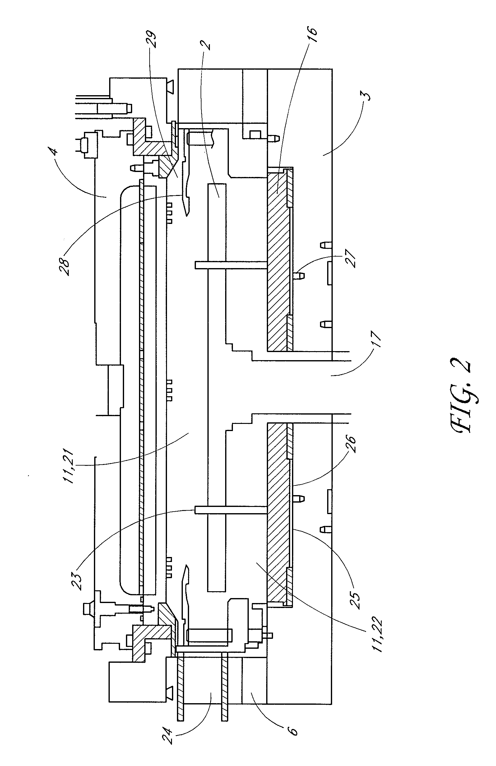
Image

Examples
example 1
[0106]Under the substantially same conditions as in Comparative Example 1 except that a ceramic material was located at the bottom surface of the chamber interior below the heater top surface and adjacent to the bottom aluminum surface.
[0107]A deposition rate was evaluated in the same way as in Comparative Example 1.
[0108]Ceramic material:
[0109]The diameter of the ceramic material: 360 mm
[0110]The thickness of the ceramic material: 26 mm
[0111]The material of the ceramic material: Al2O3
[0112]The diameter of the susceptor: 340 mm
[0113]The diameter of the shower head: 350 mm
[0114]Process conditions:
[0115]Precursor: Cyclopentene: 200 sccm
[0116]He supplied to vaporizer: 500 sccm
[0117]Ar supplied to the reactor: 1700 sccm
[0118]Process gas He supplied to the reactor: 1300 sccm
[0119]RF Power (13.56 MHz): 2300 W
[0120]Pressure: 733 Pa
[0121]Deposition time: 15.5 sec
[0122]Deposited film properties:
[0123]Deposition Rate: 790 nm / min
[0124]Thickness: 200 nm
[0125]Reflective Index (n) @633 nm: 1.88
[...
example 2
[0157]Under the substantially same conditions as in Comparative Example 2 except that the ceramic material used in Example 1 was located at the bottom surface of the chamber interior below the heater top surface and adjacent to the bottom aluminum surface. An accumulated film thickness was evaluated in the same way as in Comparative Example 2.
[0158]Process conditions:
[0159]Precursor: Cyclopentene: 200 sccm
[0160]He supplied to vaporizer: 500 sccm
[0161]Ar supplied to the reactor: 1700 sccm
[0162]Process gas He supplied to the reactor: 1300 sccm
[0163]RF Power (13.56 MHz): 2300 W
[0164]Pressure: 733 Pa
[0165]Deposition time: 15.5 sec
[0166]Deposited film properties:
[0167]Deposition Rate: 790 nm / min
[0168]Thickness: 200 nm
[0169]Reflective Index (n) @633 nm: 1.88
[0170]Extinction Coefficient (k) @633 nm: 0.09
[0171]Stress: −288 MPa
[0172]Accumulated film thickness: <2 nm (Residues can not be identified from visual inspection). No unwanted residues were observed on the wafer chip.
[0173]As compared...
PUM
| Property | Measurement | Unit |
|---|---|---|
| thickness | aaaaa | aaaaa |
| diameter | aaaaa | aaaaa |
| diameter | aaaaa | aaaaa |
Abstract
Description
Claims
Application Information