Integrated semiconductor light emitting device and method for manufacturing same

a light-emitting device and semiconductor technology, applied in semiconductor/solid-state device manufacturing, semiconductor devices, electrical devices, etc., can solve the problems of inability to achieve suitable integration structures aiming at plane light sources, and achieve the effects of reducing manufacturing costs, improving light-extraction efficiency, and improving light-extraction efficiency

Inactive Publication Date: 2009-12-24
MITSUBISHI CHEM CORP
View PDF5 Cites 34 Cited by
  • Summary
  • Abstract
  • Description
  • Claims
  • Application Information

AI Technical Summary

Benefits of technology

[0042]According to the present invention, there can be provided an integrated compound semiconductor light-emitting-device having a suitable configuration for emitting light as a large-area plane light source, as well as its manufacturing method.
[0043]In particular, according to the present invention, blue or ultraviolet plane-like emission with relatively higher uniformity in emission intensity can be realized even when an area of a light-emitting-device is more than several cm2. Furthermore, since the present invention is a flip-chip type light-emitting-device which can be mounted on a submount, adequate heat dissipation and higher light-extraction efficiency can be ensured.
[0044]In the present invention, the light-emitting-unit separation-trench is not formed by removing all layers including a buffer layer, light-emitting-units are placed close to each other while being electrically separated each other. This is very advantageous in increasing integration and emitting light as a large-area plane light source. Furthermore, since the degradation in a portion does not influence the whole device, the device is excellent in reliability. In addition, the light-emitting-unit separation-trench needs to be formed up to only a part of the buffer layer having sufficient electrical resistivity, which is present in common to light-emitting-units. There is no need to consider the requirement for etching such a depth as to reach a substrate and the sufficient thick buffer layer can be employed, which enables improvement of the crystallinity of a light emitting element part. This is preferable for higher output in a light-emitting-device. Also, it is preferable in shortness of the etching time.

Problems solved by technology

As above, while there has been proposed a method of forming a plurality of light-emitting-units on a same substrate, they are by no means suitable structures for integration aiming a plane light source.

Method used


Image

  • Integrated semiconductor light emitting device and method for manufacturing same
  • Integrated semiconductor light emitting device and method for manufacturing same
  • Integrated semiconductor light emitting device and method for manufacturing same

Examples


example

[0795]There will be described the present invention with reference to examples. Materials, amounts, proportions, specific processes and process orders in the following examples may be appropriately modified without departing from the scope of the invention. The scope of this invention should not be interpreted to be limited to the specific examples described below. Furthermore, in the drawings referred in the following examples, some sizes are deliberately changed to help understanding the structures, but practical dimensions are as indicated in the following description.

Examples of the Invention in Relation to Section A

example a-1

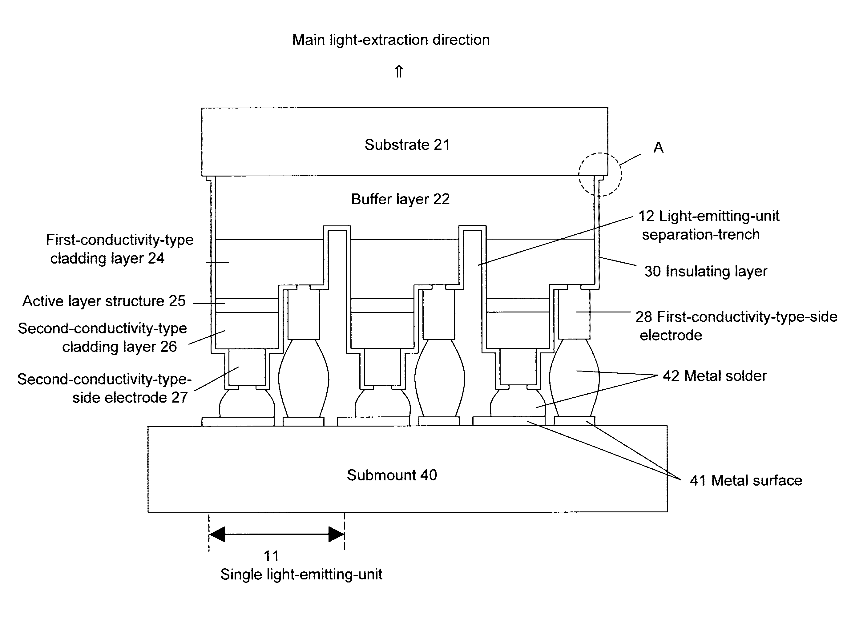
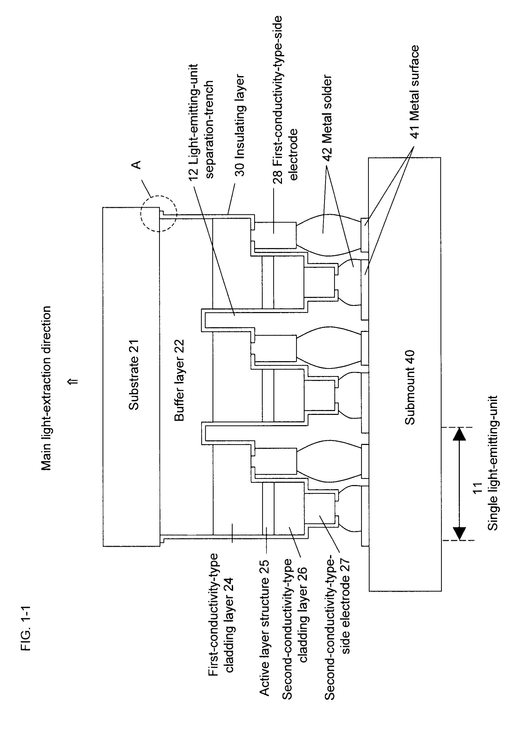
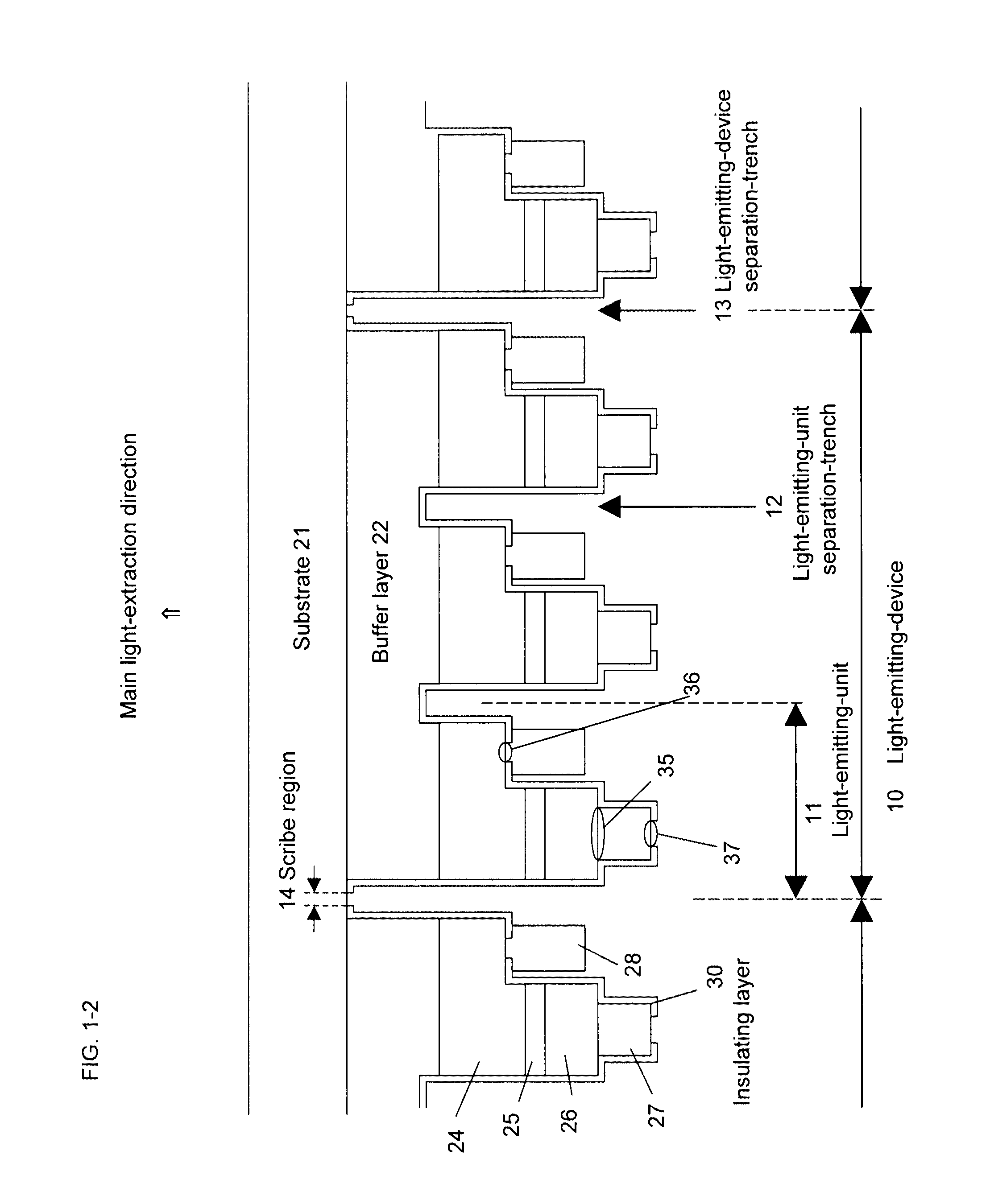
[0796]The light-emitting-device shown in FIG. 1-15 was manufactured by the following procedure. FIGS. 1-6 to 10, 12 and 14 will be referred to as a related process drawing.

[0797]First was prepared a c+ plane sapphire substrate 21 with a thickness of 430 μm, on which an undoped GaN layer with a thickness of 10 nm was formed by growing at a low temperature by MOCVD as a first buffer layer 22a; and then an undoped GaN layer with a thickness of 4 μm was deposited at 1040° C. as a second buffer layer 22b.

[0798]Then, a Si-doped (Si concentration: 1×1018 cm−3) GaN layer was formed to 2 μm as a first-conductivity-type (n-type) second cladding layer 24b; a Si-doped (Si concentration: 3×1018 cm−3) GaN layer was formed to 0.5 μm as a first-conductivity-type (n-type) contact layer 24c; and then a Si-doped (Si concentration: 1.5×1018 cm−3) Al0.15Ga0.85N layer was formed to 0.1 μm as a first-conductivity-type (n-type) first cladding layer 24a. Then, an active layer structure 25 was formed by dep...

example a-2

[0817]The procedure in Example A-1 was repeated, except that after depositing the buffer layer 22, a thin-film crystal layer was deposited as described below. Specifically, an undoped GaN was formed at 1040° C. to a thickness of 4 μm as a second buffer layer 22b as described in Example A-1, and then a Si-doped (Si concentration: 5×1018 cm−3) GaN layer was formed to 4 μm as a first-conductivity-type (n-type) second cladding layer 24b; a Si-doped (Si concentration: 8×1018 cm−3) GaN layer was formed to 0.5 μm as a first-conductivity-type (n-type) contact layer 24c; and then a Si-doped (Si concentration: 5.0×1018 cm−3) Al0.10Ga0.90N layer was formed to 0.1 μm as a first-conductivity-type (n-type) first cladding layer 24a. Then, an active layer structure 25 were formed by depositing alternately undoped GaN layer to a thickness of 13 nm at 850° C. as a barrier layer and undoped In0.1Ga0.9N layer to a thickness of 2 nm at 720° C. as a quantum well layer such that eight quantum well layers ...


PUM


Abstract

An integrated compound semiconductor light-emitting-device capable of emitting light as a large-area plane light source, exhibiting excellent in-plane uniformity in an emission intensity is provided. The light-emitting-device comprising a plurality of light-emitting-units formed over a substrate, wherein the light-emitting-unit has a compound semiconductor thin-film crystal layer 24, 25, 26 a first and a second-conductivity-type-side electrode 27, 28; a main light-extraction direction is the side of the substrate, and the first and the second-conductivity-type-side electrode are formed on the opposite side to the light-extraction direction; the light-emitting-units are electrically separated each other by a light-emitting-unit separation-trench which is formed by removing the thin-film crystal layer from the surface to an inside portion of the buffer layer.

Description

TECHNICAL FIELD[0001]The present invention relates to a compound semiconductor light-emitting device, particularly a light-emitting diode (LED) having a GaN material. As used herein, the term “light-emitting diode” or “LED” encompasses light-emitting elements in general which include a laser diode and a superluminescent diode and the like.BACKGROUND ART[0002]Electron devices and light-emitting-devices having a Group III-V compound semiconductor are well-known. In particular, there have been practically used as a light-emitting-device an AlGaAs or AlGaInP material formed on a GaAs substrate for red luminescence and a GaAsP material formed on a GaP substrate for orange or yellow luminescence. An infrared light-emitting-device using an InGaAsP material on an InP substrate is also known.[0003]As the types of these devices, a light-emitting diode utilizing spontaneous emissive light (light-emitting diode: LED), a laser diode having an optical feedback function for deriving an induced emi...

Claims


Application Information

Patent Timeline
Patent Type & Authority Applications(United States)
IPC IPC(8): H01L33/00
CPCH01L27/153H01L2224/16225H01L2224/1403
Inventor HORIE, HIDEYOSHI
Owner MITSUBISHI CHEM CORP
Why Eureka
Try Eureka