The latter aspect is especially important since, in modern semiconductor facilities, equipment is required which is extremely cost-intensive and represents the dominant part of the total production costs.
This problem is even exacerbated in current developments striving to increase the size of substrates, on which a moderately high number of such integrated circuits are commonly processed, so that failure in a
single process step may possibly entail the loss of a large number of products.
A corresponding
process control, however, is not practical, since measuring the effects of certain processes may require relatively long measurement times, frequently ex situ, or may even necessitate the destruction of the sample.
Moreover, immense effort, in terms of time and equipment, would have to be made on the
metrology side to provide the required measurement results.
Furthermore, many of the complex mutual dependencies of the various processes are typically not known, so that an a priori determination of respective “optimum” process specifications may be difficult.
Nevertheless, in total, a large number of dummy substrates or
pilot substrates may be necessary to adjust process parameters of respective process tools, wherein tolerable parameter drifts during the process have to be taken into consideration when designing a process sequence, since such parameter drifts may remain undetected over a long time period or may not be efficiently compensated for by SPC techniques.
Although significant advances in providing enhanced
process control strategies have been made, process variations may nevertheless occur during the complex interrelated manufacturing sequences, which may be caused by the plurality of individual process steps, which may affect the various materials in a more or less pronounced manner.
On the other hand, the introduction of
copper into semiconductor manufacturing strategies may be associated with a plurality of problems, such as sensitivity of exposed
copper surfaces with respect to
reactive components, such as
oxygen,
fluorine and the like, the increased
diffusion activity of
copper in a plurality of materials typically used in semiconductor devices, such as
silicon,
silicon dioxide, a plurality of low-k
dielectric materials and the like, copper's characteristic of generating substantially no volatile byproducts on the basis of typically used
plasma-enhanced etch processes, and the like.
Consequently, a plurality of highly complex processes, such as the deposition of sophisticated material stacks for forming the interlayer
dielectric material including low-k dielectrics, patterning the dielectric material, providing appropriate barrier and seed materials,
filling in the copper material, removing any excess material and the like, may be required for forming sophisticated metallization systems wherein the mutual interactions of these processes may be difficult to assess, in particular, as material compositions and process strategies may frequently change in view of further enhancing overall performance of the semiconductor devices.
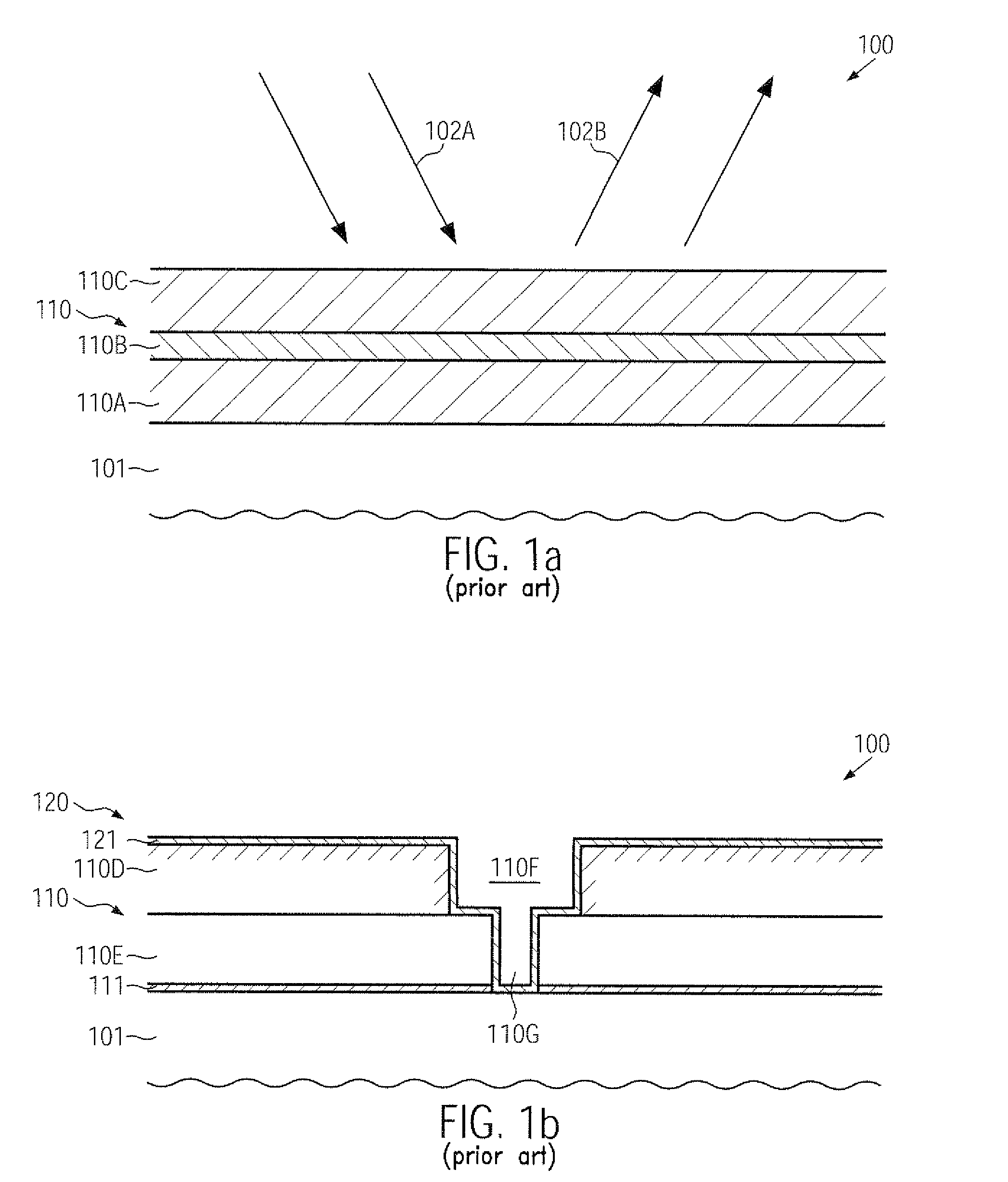
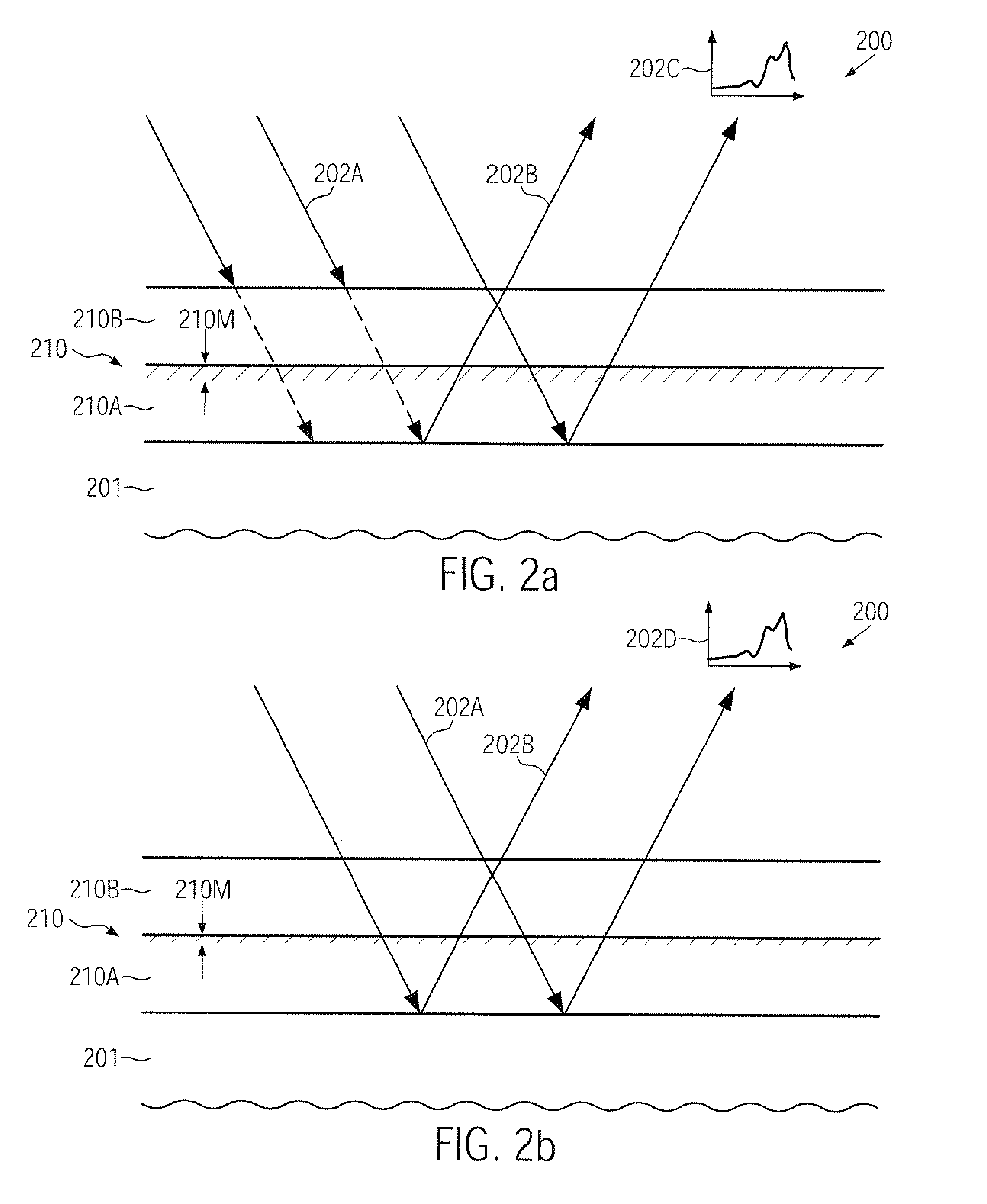
However, the conventionally applied optical measurement techniques may provide information about material characteristics which may vary in a more or less step-like manner, such as a pronounced change of the index of
refraction at interfaces between the various
layers 110A, 10B, 110C, which may be very convenient in determining the optical thickness of the materials 110 but which may not provide information with respect to a more or less gradually varying material characteristic of one or more of the
layers 110.
For example, it may be very difficult to determine a gradual variation within one of the
layers 110 in different semiconductor devices or device areas on the basis of conventionally applied optical measurement techniques.
For example, the material modification or damaging of the layer 110D may result in a reduced adhesion and / or
diffusion blocking effect of the barrier material 121, which may compromise the overall reliability of the metallization
system 120.
In other cases, during the removal of excess material of the copper and the barrier material 121 after the electrochemical deposition of the copper material, the damaged areas of the layer 110D may have an influence on the removal conditions, which in turn may also negatively affect the overall characteristics of the resulting metallization
system 120.
Since the degree of material modification may gradually vary due to even minor process variations during the complex sequence of manufacturing processes involved, in particular in patterned device structures, it may be extremely difficult to obtain a
quantitative measure of the degree of damage on the basis of optical measurement techniques used in a conventional context.
However, due to the destructive nature of the analysis techniques involved, only a very limited amount of measurement data may be gathered, thereby contributing to a less efficient overall process control.
Furthermore, due to the external analysis technique including sophisticated
sample preparation and the like, a significant amount of
delay may be involved in obtaining the measurement data, thereby also contributing to a less efficient control mechanism for the manufacturing sequence for forming the metallization
system 120.

