Method for improving inversion layer mobility in a silicon carbide mosfet

a technology of metal oxide semiconductors and inversion channels, applied in the direction of semiconductor devices, electrical equipment, basic electric elements, etc., can solve the problems of low threshold voltage, inability to meet the requirements of current or future applications, etc., to achieve the effect of improving the mobility of inversion channels and low threshold voltag

Active Publication Date: 2010-01-14
UNITED MICROELECTRONICS CORP
View PDF6 Cites 18 Cited by
  • Summary
  • Abstract
  • Description
  • Claims
  • Application Information

AI Technical Summary

Benefits of technology

[0008]It is an object of the present invention to mitigate the above problem, and provide an oxide layer on the Si-face of a SiC substrate which, when used for manufacturing a semiconductor device, will result in improved inversion channel mobility, but with a sufficiently low threshold voltage.

Problems solved by technology

This means that further refinements in device design and processing are not likely to yield substantial improvements in performance.
However, this state of affairs is not acceptable for a variety of current or future applications where silicon power-devices function with heavy operating losses.
However, epitaxial layers grown on the C-face are currently not commercially available, and it is therefore desired to form the gate oxide on the Si-face.
However, SiC MOSFETs currently fabricated on the Si-face of a SiC substrate have shown very poor inversion layer mobility (˜1 cm2 / Vs), which is one hundred times lower than the expected mobility value.
This results in large power dissipation and loss of efficiency, which makes SiC MOSFETs less attractive in comparison to their Si counterparts.
The lower inversion layer mobility is primarily due to the poor interface between the gate oxide and the silicon carbide substrate through which the current conduction occurs.
However, when implementing rapid oxidation of SiC, a negative side effect is that the threshold voltage of the semiconductor device increases.

Method used


Image

  • Method for improving inversion layer mobility in a silicon carbide mosfet
  • Method for improving inversion layer mobility in a silicon carbide mosfet
  • Method for improving inversion layer mobility in a silicon carbide mosfet

Examples


Embodiment Construction

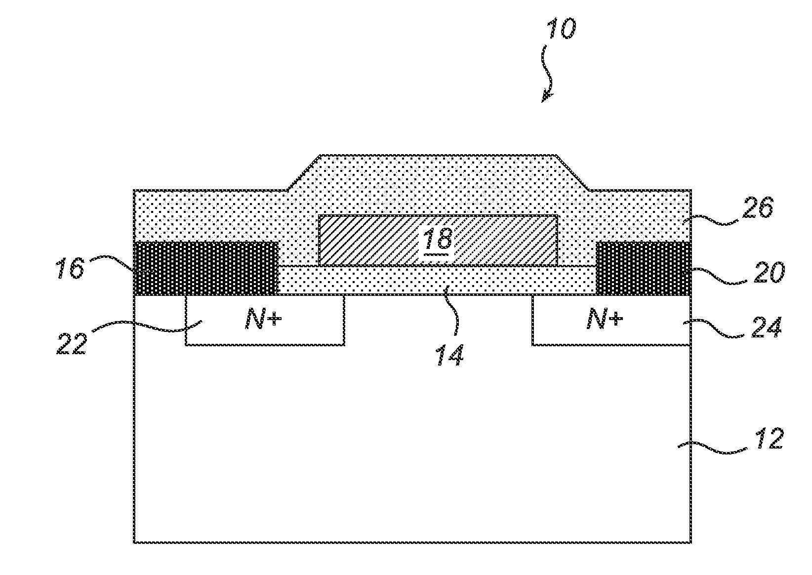
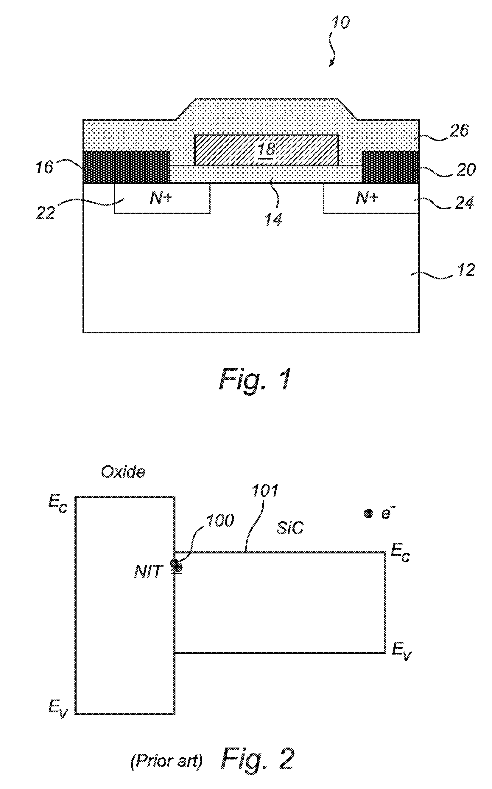
[0041]It is noted that the drawings of the invention are not necessarily to scale. The drawings are merely schematic representations, not intended to portray specific parameters of the invention. The drawings are intended to depict only typical embodiments of the invention, and therefore should not be considered as limiting the scope of the invention. In particular, the method according to the present invention is described with reference to an embodiment, in which an oxidation enhancing agent, here sodium, is introduced during oxidation in order to increase the oxidation rate to a sufficiently high level. It should be noted that it is the oxidation rate as such in combination with the hydrogen passivation that are central to the present invention. Consequently, the present invention is equally applicable to a process involving any other way of accomplishing the desired oxidation rate, such as introduction of other alkali metals, such as potassium or rubidium, introduction of other ...


PUM

PropertyMeasurementUnit
temperatureaaaaaaaaaa
interface energyaaaaaaaaaa
temperatureaaaaaaaaaa

Abstract

A method of manufacturing a semiconductor device based on a SiC substrate (12), comprising the steps of forming (201) an oxide layer (14) on a Si-terminated face of the SiC substrate (12) at an oxidation rate sufficiently high to achieve a near interface trap density below 5×1011 cm−2; and annealing (202) the oxidized SiC substrate in a hydrogen-containing environment, in order to passivate deep traps formed in the oxide-forming step, thereby enabling manufacturing of a SiC-based MOSFET (10) having improved inversion layer mobility and reduced threshold voltage. It has been found by the present inventors that the density of DTs increases while the density of NITs decreases when the Si-face of the SiC substrate is subject to rapid oxidation. According to the present invention, the deep traps formed during the rapid oxidation can be passivated by hydrogen annealing, thus leading to a significantly decreased threshold voltage for a semiconductor device formed on the oxide.

Description

TECHNICAL FIELD OF THE INVENTION[0001]The present invention generally relates to a method for improving inversion layer mobility in a silicon carbide (SiC) metal-oxide semiconductor field-effect transistor (MOSFET). In particular, the present invention relates to forming a gate oxide on the Si-face of a SiC substrate to yield a MOSFET with improved inversion layer mobility.TECHNICAL BACKGROUND[0002]Silicon (Si) is, and has been, the most popular and widely used semiconductor material for the past thirty years. During this time, Si device technology has reached an advanced level because of constant refinements and improvements. The result of this constant improvement has brought silicon power devices to such levels of efficiency that they are now approaching the theoretical maximum power limit predicted for this material. This means that further refinements in device design and processing are not likely to yield substantial improvements in performance. However, this state of affairs ...

Claims


Application Information

Patent Timeline
Patent Type & Authority Applications(United States)
IPC IPC(8): H01L29/161H01L21/18H01L21/04
CPCH01L29/66068Y10S438/931
Inventor ROEDLE, THOMAS C.SVEINBJORNSSON, ELNAR O.OLAFSSON, HALLDOR O.GUDJONSSON, GUDJON I.ALLERSTAM, CARL F.
Owner UNITED MICROELECTRONICS CORP
Why Eureka
Try Eureka