

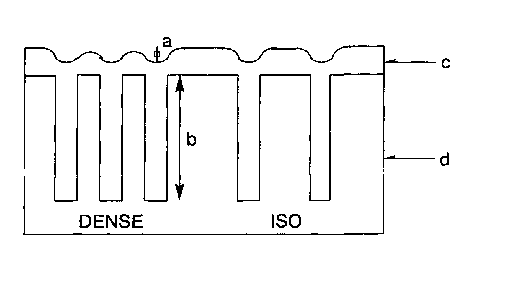
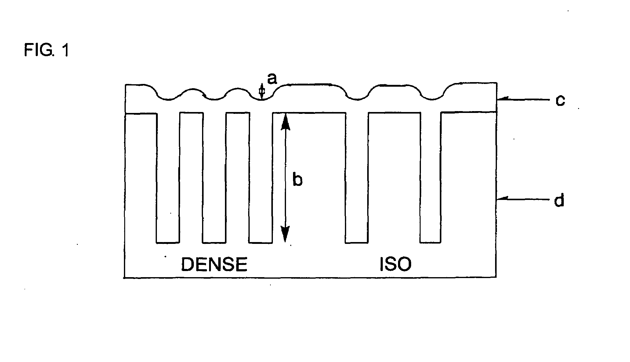
Resist underlayer film forming composition for lithography, containing aromatic fused ring-containing resin
a technology of resin and underlayer film, which is applied in the direction of basic electric elements, electrical appliances, and paper, etc., can solve the problems of large influence of diffuse reflection of activating light ray from the substrate or of standing wave, difficult to obtain film thickness of resist pattern sufficient for processing the substrate, and large influence of standing wave reflection from the substrate. achieve satisfactory etching resistance and efficient suppression of reflection from the substra
- Summary
- Abstract
- Description
- Claims
- Application Information
AI Technical Summary
Benefits of technology
Problems solved by technology
Method used
Image

Examples
synthesis example 1
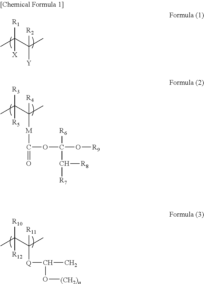
[0135]30 g of 2-vinyl naphthalene, 3.5 g of glycidyl methacrylate and 4.5 g of 1-butoxyethyl methacrylate were dissolved in 112 g of cyclohexanone and then, the inside of a flask was purged with nitrogen, followed by elevating the temperature to 60° C. After elevating the temperature, 1.9 g of azobis-isobutylonitrile dissolved in 48 g of cyclohexanone were added to the reaction solution under nitrogen pressure and the reaction was effected at 60° C. for 24 hours. The reaction solution was cooled and then charged into methanol and a polymer was reprecipitated. The obtained polymer was dried by heating to obtain a polymer represented by Formula (7-1). The obtained polymer had a weight average molecular mass Mw of 12,000 (as converted into polystyrene). In Formula (7-1), when the total number of all unit structures constituting the polymer is assumed to be 1.0, the ratio of the number of unit structures containing 2-vinyl naphthalene, the ratio of the number of unit structures containi...
synthesis example 2
[0136]20 g of 2-vinyl naphthalene, 8.1 g of styrene, 3.7 g of glycidyl methacrylate and 4.1 g of 1-ethoxyethyl methacrylate were dissolved in 106 g of cyclohexanone and then the inside of a flask was purged with nitrogen, followed by elevating the temperature to 60° C. After elevating the temperature, 1.8 g of azobis-isobutylonitrile dissolved in 45 g of cyclohexanone were added to the reaction solution under nitrogen pressure and the reaction was effected at 60° C. for 24 hours. The reaction solution was cooled and then charged into methanol and a polymer was reprecipitated. The obtained polymer was dried by heating to obtain a polymer represented by Formula (7-2). The obtained polymer had a weight average molecular mass Mw of 11,000 (as converted into polystyrene).
[0137]In Formula (7-2), when the total number of all unit structures constituting the polymer is assumed to be 1.0, the ratio of the number of unit structures containing 2-vinyl naphthalene, the ratio of the number of un...
synthesis example 3
[0138]30 g of acenaphthylene and 9.2 g of 1-butoxyethyl methacrylate were dissolved in 115 g of cyclohexanone and then the inside of a flask was purged with nitrogen, followed by elevating the temperature to 60° C. After elevating the temperature, 2.0 g of azobis-isobutylonitrile dissolved in 49 g of cyclohexanone were added to the reaction solution under nitrogen pressure, and the reaction was effected at 60° C. for 24 hours. The reaction solution was cooled and then charged into methanol and a polymer was reprecipitated. The obtained polymer was dried by heating to obtain a polymer represented by Formula (4-2). The obtained polymer had a weight average molecular mass Mw of 10,000 (as converted into polystyrene).
[0139]In Formula (4-2), when the total number of all unit structures constituting the polymer is assumed to be 1.0, the ratio of the number of unit structures containing acenaphthylene and the ratio of the number of unit structures containing 1-butoxyethyl methacrylate were...
PUM
| Property | Measurement | Unit |
|---|---|---|
| wavelength | aaaaa | aaaaa |
| wavelength | aaaaa | aaaaa |
| wavelength | aaaaa | aaaaa |
Abstract
Description
Claims
Application Information