

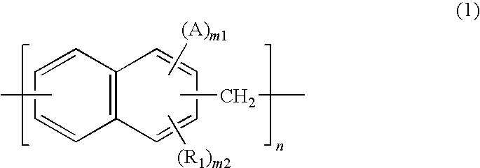
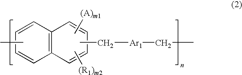
Coating-type underlayer coating forming composition for lithography containing naphthalene resin derivative
a technology of naphthalene resin and coating type, applied in the direction of photosensitive materials, instruments, photomechanical equipment, etc., can solve the problems of low resolution, difficult to obtain a film thickness of resist pattern sufficient for substrate processing, and the influence of random reflection and standing wave of actinic rays on a substrate. serious problems
- Summary
- Abstract
- Description
- Claims
- Application Information
AI Technical Summary
Benefits of technology
Problems solved by technology
Method used
Image


Examples
synthetic example 1
[0044]After 50.0 g of the compound of formula (158) (manufactured by Daicel Chemical Industries, Ltd., trade name: EHPE3150) and 57.4 g of 9-anthracene carboxylic acid were dissolved in 435.7 g of propylene glycol monomethyl ether, 1.5 g of benzyl triethyl ammonium was added, and the resulting mixture was refluxed for 24 hours to obtain a solution of the polymer compound of formula (159). GPC analysis of the resulting polymer compound showed that it had a weight average molecular weight of 3000 in terms of standard polystyrene.
[0045]
synthetic example 2
[0046]After 50.0 g of the compound of formula (160) (manufactured by Nippon Steel Chemical Co., Ltd., trade name: ESN175S) and 37.3 g of 9-anthracene carboxylic acid were dissolved in 353.0 g of propylene glycol monomethyl ether, 1.0 g of benzyl triethyl ammonium was added, and the resulting mixture was refluxed for 24 hours to obtain a solution of the polymer compound of formula (161). GPC analysis of the resulting polymer compound showed that it had a weight average molecular weight of 2500 in terms of standard polystyrene.
[0047]
synthetic example 3
[0048]After 50.0 g of the compound of formula (162) (manufactured by Nippon Steel Chemical Co., Ltd., trade name: ESN375) and 60.1 g of 9-anthracene carboxylic acid were dissolved in 447.0 g of propylene glycol monomethyl ether, 1.6 g of benzyl triethyl ammonium was added, and the resulting mixture was refluxed for 24 hours to obtain a solution of the polymer compound of formula (163). GPC analysis of the resulting polymer compound showed that it had a weight average molecular weight of 2500 in terms of standard polystyrene.
[0049]
PUM
| Property | Measurement | Unit |
|---|---|---|
| wavelength | aaaaa | aaaaa |
| wavelength | aaaaa | aaaaa |
| wavelength | aaaaa | aaaaa |
Abstract
Description
Claims
Application Information