Photoresist developing solution

A technology of photoresist and developer, applied in optics, photography, optomechanical equipment, etc., can solve problems such as increased scum, and achieve high dimensional accuracy and high industrial use value

Inactive Publication Date: 2010-02-24
TOKUYAMA CORP
View PDF3 Cites 9 Cited by
  • Summary
  • Abstract
  • Description
  • Claims
  • Application Information

AI Technical Summary

Problems solved by technology

However, as the thickness of the photoresist layer becomes thicker, the amount of the resist component dissolved in the developer increases, so there is a problem such as increased generation of scum, and it is difficult to form a fine resist pattern with high precision. When the above developer develops a resist layer having a thickness of 3 μm or more, the generation of scum increases, and it is necessary to improve the development characteristics

Method used


Image

  • Photoresist developing solution
  • Photoresist developing solution
  • Photoresist developing solution

Examples


manufacture example 1~9 and comparative manufacture example 1~4

[0102] A 20.0% by mass TMAH aqueous solution (manufactured by Tokuyama Co., Ltd., trade name SD-20) was diluted with ultrapure water to prepare a 3.0% by mass TMAH aqueous solution, and Table 1 (Manufacturing Examples 1-4), Various surfactants were prepared in amounts (mass %) shown in Table 2 (Production Examples 5 to 9) and Table 3 (Comparative Production Examples 1 to 4) to prepare various photoresist developing solutions.

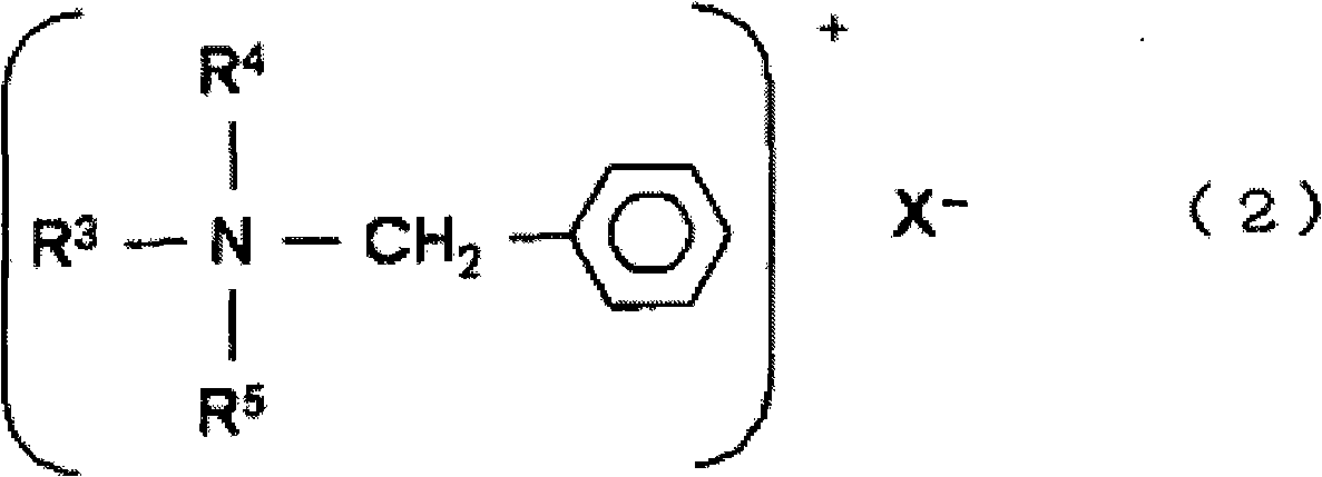
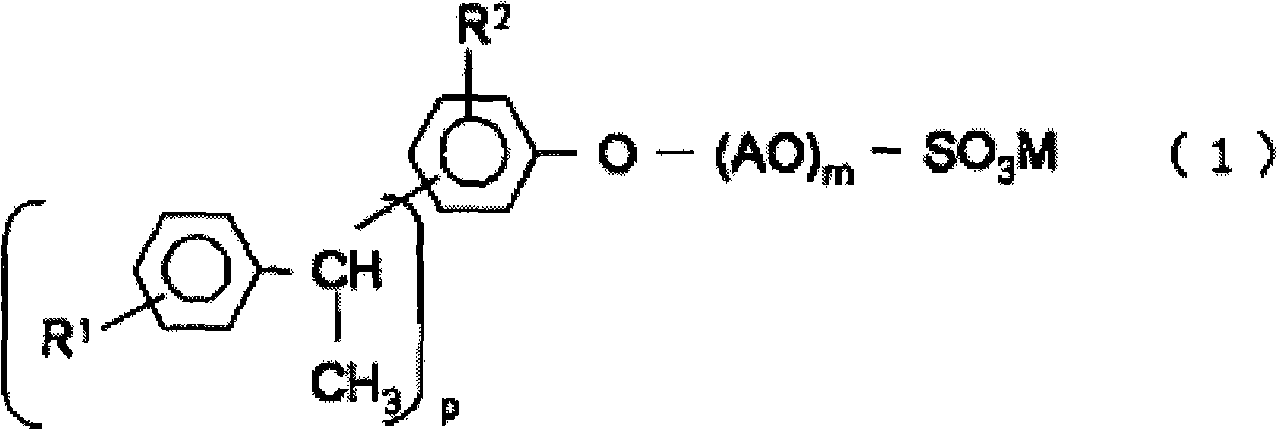
[0103] In addition, in comparative manufacture example 1, neither anionic surfactant nor cationic surfactant was used. In addition, the anionic surfactant was treated with a cation exchange resin, and the total concentration of sodium ions and potassium ions in the anionic surfactant (100% conversion) was adjusted to be 10 ppm or less before use. Tables 1, 2, and 3 also show the pH, concentrations of sodium ions and potassium ions of these various developers.

[0104]

[0105]

[0106]

Embodiment 1~9 and comparative example 1~5

[0108] As positive type resists for thick film formation, the following two types of resists were prepared.

[0109] Phenolic-diazonaphthoquinone positive resist:

[0110] Resin composition: thermoplastic phenolic resin (alkali-soluble resin)

[0111] Sensitizer: naphthoquinone diazide

[0112] Chemically Amplified Resist (Positive Type):

[0113] A photoresist containing a polymethacrylic resin having a carboxylic acid protected with an ester group as a resin component, polyhydroxystyrene as an alkali-soluble resin, and an acid generator

[0114] A 4-inch silicon wafer was prepared, and the wafer was washed with sulfuric acid-hydrogen peroxide (volume ratio 4:1). Then bake at 200° C. for 60 seconds on a hot plate.

[0115] Next, the above-mentioned positive-type photoresist was coated on the silicon wafer using a spin coater to form a positive-type photoresist layer having a film thickness of 3.5 μm.

[0116] After irradiating g, h, and i rays with a wavelength of 300 to...

Embodiment 10~18 and comparative example 6~9

[0132] Except that the film thickness of the applied positive photoresist was 20.0 μm, development was carried out using various developing solutions in the same manner as in the above-mentioned Examples and Comparative Examples to obtain a contact hole pattern with a width of 20 μm in the pattern gap. Do the same evaluation. The results are shown in Table 5.

[0133] table 5

[0134]

[0135] As shown in the experimental results in Table 4 and Table 5, when using the developer solution of the present invention for development (Examples 1-18), when the thickness of the photoresist layer is 3 μm or more, using a common photoresist and chemical amplification When a photoresist layer was formed with any type of photoresist, no scum was generated, and the pattern shape was also good.


PUM

PropertyMeasurementUnit
thicknessaaaaaaaaaa
widthaaaaaaaaaa
thicknessaaaaaaaaaa

Abstract

The invention provides a developing solution which can be used suitably for the development of a thick resist comprising a chemically amplified resist. Disclosed is a photoresist developing solution comprising an aqueous quaternary ammonium compound solution containing an anionic surfactant and a cationic surfactant, wherein the anionic surfactant is represented by the formula (1) and is containedin an amount of 0.1 to 5% by mass and the cationic surfactant is contained in an amount of 0.01 to 2% by mass relative to 100% by mass of the total mass of the photoresist developing solution. (1) wherein R<1> represents a hydrogen atom or a methyl group; R<2> represents a hydrogen atom or an alkyl group having 1 to 4 carbon atoms; A represents an alkylene group having 1 to 4 carbon atoms, provided that AO's may be the same as each other or may be a combination of different two or more groups in the molecule; p is an integer of 1 to 3; m is an integer of 5 to 30; and M represents a hydrogen atom or an ammonium ion.

Description

technical field [0001] The present invention relates to a new type of photoresist developer used in the manufacture of semiconductor devices, flat panel displays (FPD), circuit boards, magnetic heads, etc. A photoresist developing solution that can be preferably used for developing a photoresist. Background technique [0002] In a wide range of fields including the manufacture of semiconductor integrated circuits such as LSIs, the manufacture of FPD display surfaces, and the manufacture of circuit substrates such as magnetic heads, the importance of precision processing technologies for forming fine elements and performing microfabrication has increased. Among such precision processing techniques, a processing method called photo fabrication (photo fabrication) has become the mainstream. Photoprocessing refers to applying a photosensitive resin composition called photoresist on the surface of a workpiece to form a coating film (resist layer) for exposure, and using a develo...

Claims


Application Information

Patent Timeline
Patent Type & Authority Applications(China)
IPC IPC(8): G03F7/32G03F7/023G03F7/039H01L21/027
CPCG03F7/322G03F7/0392
Inventor 东野诚司名塚康隆
Owner TOKUYAMA CORP
Why Eureka
Try Eureka