Etching solution composition for metal thin film consisting primarily of copper
一种蚀刻液、组合物的技术,应用在蚀刻液组合物领域,能够解决易产生颗粒、需要劳动力、基板密合性恶化等问题,达到优异图案形状、高蚀刻活性、抑制蚀刻速度的效果
- Summary
- Abstract
- Description
- Claims
- Application Information
AI Technical Summary
Problems solved by technology
Method used
Image
Examples
Embodiment 1~2
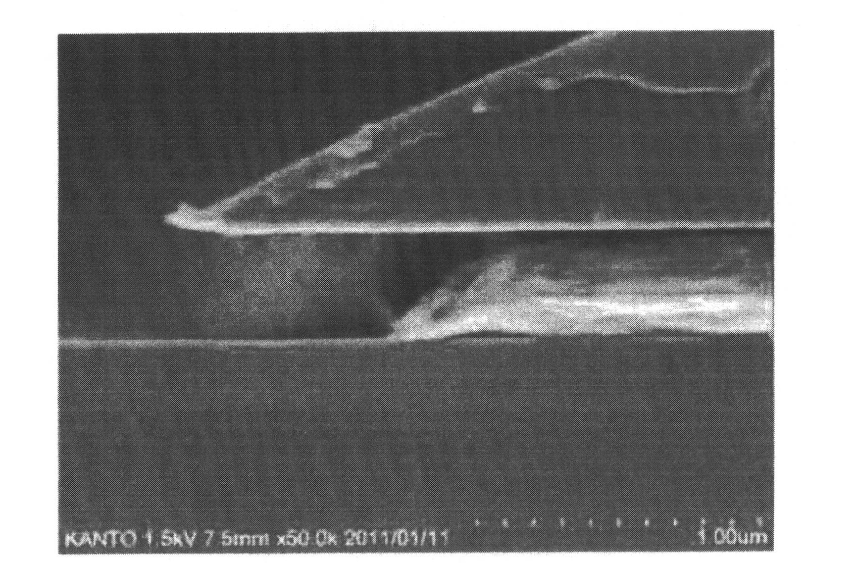
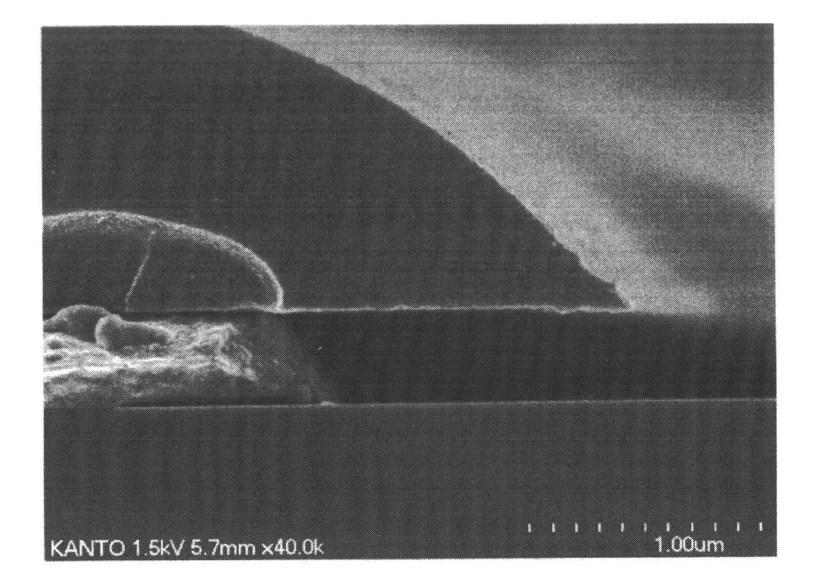
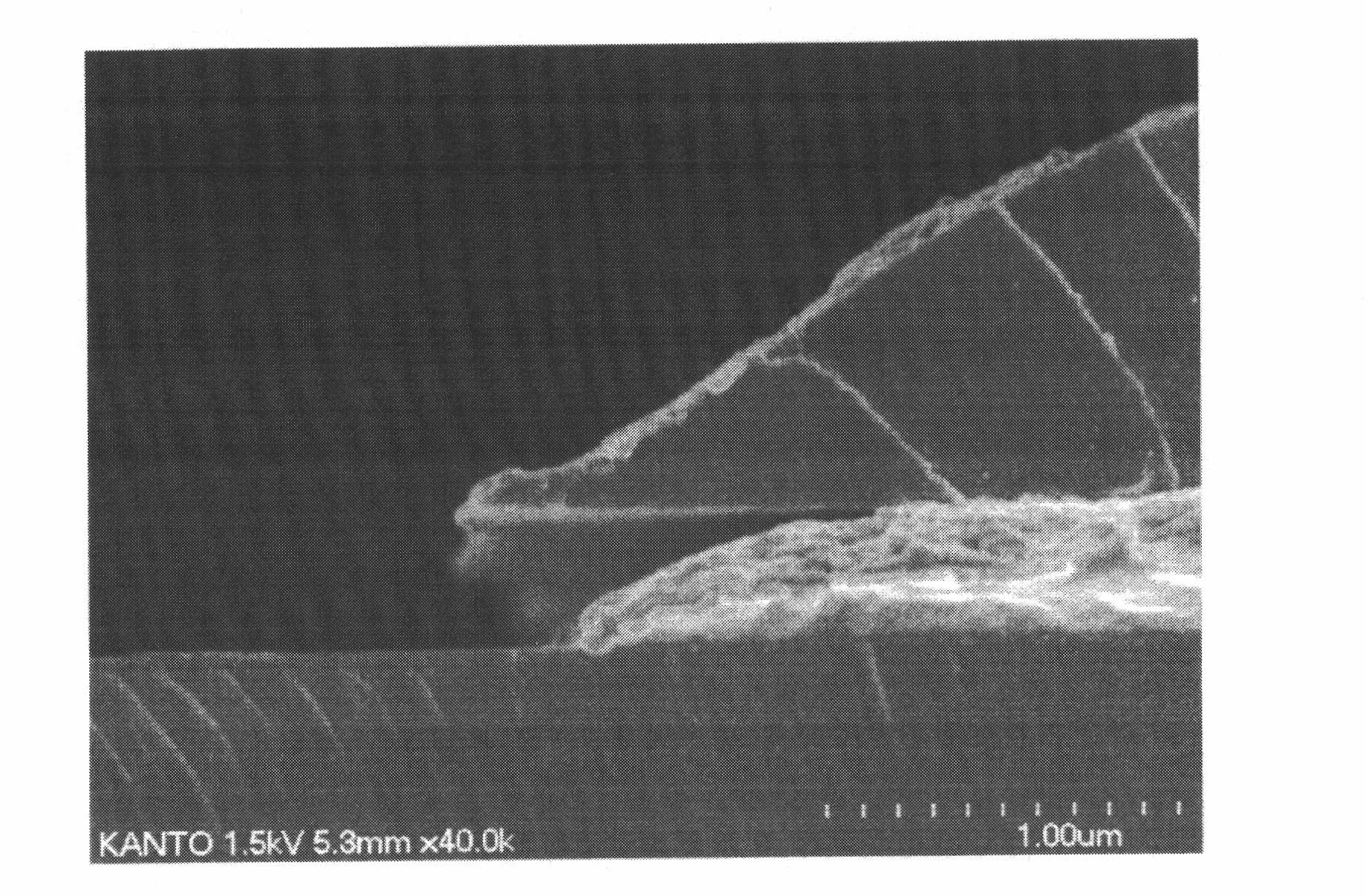
[0079] Thick film formed on glass substrate Cu alloy (Cu-Mg-Al), film thickness After forming a Cu film, a resist pattern was formed and immersed in the etching solution in Table 1 (Examples 1-2) at a liquid temperature of 30° C. for 1.5 times the appropriate etching time. Thereafter, the washed and dried substrate was observed under a microscope, and the amount of side etching, tapered shape, and residue after etching were evaluated.
[0080] The results are shown in Table 1.
[0081] Table 1
[0082] Cu / CuMgAl / Glass substrate
[0083]
Embodiment 3~4
[0085] Thick film formed on glass substrate Cu alloy (Cu-Mg-Al-O), film thickness After forming a Cu film, a resist pattern was formed and immersed in the etching solution in Table 2 (Examples 3-4) at a liquid temperature of 30°C for 1.5 times the appropriate etching time. Thereafter, the washed and dried substrate was observed under a microscope, and the amount of side etching, tapered shape, and residue after etching were evaluated.
[0086] The results are shown in Table 2.
[0087] Table 2
[0088] Cu / CuMgAlO / glass substrate
[0089]
[0090] The etchant composition of the present invention has a specific composition due to phosphoric acid, nitric acid, and acetic acid, so that a metal laminate film formed of copper / copper alloy or copper alloy / copper / copper alloy can be formed with almost no etching residue and good precision. Etching process can be performed accurately to obtain an excellent pattern shape, and a flat panel display device with high yield a...
Embodiment 5~8
[0092] Thick film formed on glass substrate After the Cu alloy film (Cu-Mg-Al), the film thickness is formed After the Cu film was formed, the substrate with the resist pattern and the glass substrate were formed with a film thickness Cu alloy oxide film (Cu-Mg-Al-O), followed by the formation of film thickness Cu alloy film (Cu-Mg-Al), forming a film thickness After forming the film of Cu, a resist pattern is formed. For the etching solution in Table 1 (Example 1), the stirrer is stirred under the condition of no stirring or the condition of the number of revolutions of 700rpm. 1.5 times the time of immersion. Thereafter, the washed and dried substrate was observed under a microscope, and the amount of side etching, tapered shape, and residue after etching were evaluated. The results are shown in Table 3.
[0093] table 3
[0094] Cu / CuMgAl / glass substrate, Cu / CuMgAl / CuMgAlO / glass substrate
[0095]
Substrate
to stir
Side etching amount
co...
PUM
| Property | Measurement | Unit |
|---|---|---|
| angle | aaaaa | aaaaa |
Abstract
Description
Claims
Application Information


