[0012]The present invention makes it possible to suppress the short channel effect and to obtain a high drive current with a
semiconductor device having MISFET in which a material with a high mobility and high dielectric constant, such as germanium, is used for the channel.BEST
MODES FOR CARRYING OUT THE INVENTION
[0013]Hereinafter, exemplary embodiments of the present invention will be described in a concretive manner by referring to the accompanying drawings. First, a first exemplary embodiment of the present invention will be described. FIG. 1 is a sectional view showing a
semiconductor device according to the first exemplary embodiment.
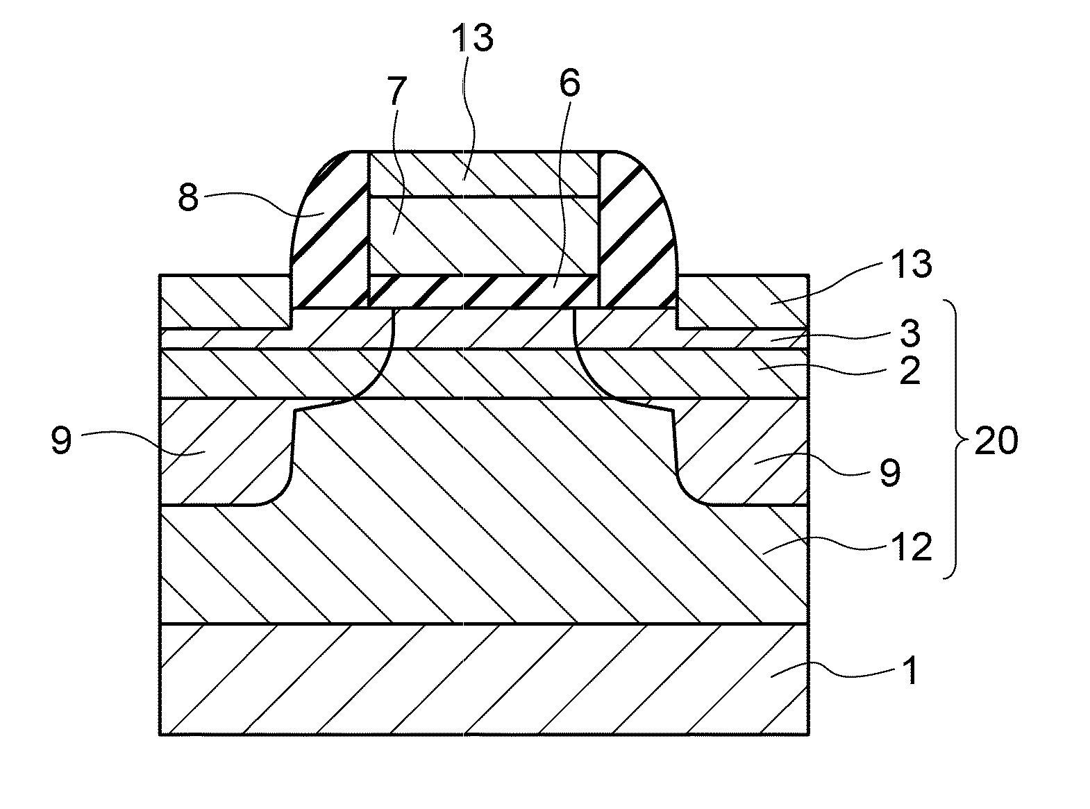
[0014]As shown in FIG. 1, a p-type well 12 is formed on a surface of a p-type silicon substrate 1. A
silicon germanium layer 2 and a germanium layer 3 are formed thereon in order from the p-type well 12 side. The germanium content of the silicon germanium layer 2 is 20-80%. Further, a preferable film thickness of the silicon germanium layer 2 is 30 nm or less, and a preferable film thickness of the germanium layer 3 is 3-40 nm. The silicon germanium layer 2 and the germanium layer 3 are formed by a CVD (
Chemical Vapor Deposition) method or an MBE (
Molecular Beam Epitaxy) method.
[0015]N-type
impurity diffusion regions 9 in a pair are formed by being isolated from each other through diffusing impurities in a part of a semiconductor region 20 that is configuredwith the p-type well 12, the silicon germanium layer 2, and the germanium layer 3. This pair of n-type
impurity diffusion regions 9 configures the source and drain of MISFET. Further, the germanium layer 3 sandwiched between the n-type
impurity diffusion regions 9 forms a channel region. A gate insulating film 6 is formed to cover the channel region between the source and the drain, and a gate
electrode 7 is formed thereon. A sidewall insulating film 8 is formed around the gate insulating film 6 and the gate
electrode 7. Further, a
silicide layer 13 is formed on the surface of the germanium layer 3 and the gate electrode 7 by
silicide chemical reaction. While an element isolation region such as a shallow trench for isolating elements of each MISFET, an interlayer insulating film such as a
silicon oxide film covering the entire MISFET, wirings for electrically connecting each MISFET and other elements and the like, etc., are formed in practice, those are omitted from the drawings.
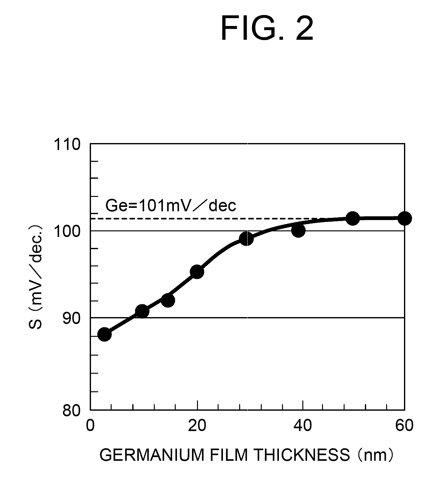
[0016]In the followings, the reason for setting the film thickness of the germanium layer as 3-40 nm in this exemplary embodiment will be described. In general, when forming the germanium layer for configuring the channel region of the MISFET, germanium is epitaxial-grown on the silicon substrate. At that time, a compression
distortion is applied to the germanium layer, due to the fact that the
grating constant of silicon and that of germanium are different. When the film thickness of the germanium layer is increased,
dislocation is introduced within the germanium layer, which results in causing a bad influence upon the performance of the MISFET, such as an increase in the leak current. Therefore, it is necessary to form the germanium layer in a thickness with which
dislocation is not introduced, and the critical film thickness thereof is about 2 nm. In the meantime, carriers are distributed in the range mainly about 3 nm below the gate insulating film in the channel region of the MISFET, so that the carriers are to run on the silicon layer whose mobility is lower than that of germanium. This causes deterioration of the drive current.
[0017]A following fact is reported in a literature by J. Nakatsuru et al., “Growth of high quality Ge epitaxial layer on Si(100) substrate using ultra thin Si0.5Ge0.5 buffer”, MRS Fall Meeting Abstracts EE7.24, pp. 758-763, 2005. In the literature, the author et al., epitaxial-grew germanium on a silicon germanium layer as an intermediate layer formed on a silicon layer. As a result, obtained was such an experimental result that even though the germanium layer on the top layer is relaxed because
dislocation is introduced in the silicon germanium layer, most of the dislocation remains in the vicinity of the interface between the germanium layer and the silicon germanium layer and does not propagate to the surface of the relaxed germanium layer.

