Eureka AIR delivers breakthrough ideas for toughest innovation challenges, trusted by R&D personnel around the world.

Photoconductive device

Inactive Publication Date: 2010-03-04
CANON KK
View PDF14 Cites 21 Cited by
  • Summary
  • Abstract
  • Description
  • Claims
  • Application Information

AI Technical Summary

Benefits of technology

[0007]Even in LT-GaAs, as described above, application of a voltage of about 100 V may cause no damage to the photoconductive portion in the case where the gap between electrodes is about 5 μm. However, application of a higher voltage often causes damage thereto. In this way, regardless of the properties of the material used for the photoconductive portion, application of a high voltage for obtaining the higher intensity in a terahertz wave may cause damage to the photoconductive portion.
[0013]The photoconductive device of the present invention makes it possible to increase resistance between the antenna portion of the first conductive portion and the antenna portion of the second conductive portion separated via the gap to be able to withstand a higher voltage. Thus, the photoconductive device allows a higher voltage to be applied between two conductive portions. Accordingly, for example, the photoconductive device makes it possible to increase intensity of an obtainable maximum terahertz wave.

Problems solved by technology

However, applying a too high voltage to perform irradiation of a laser light causes an excessive current to flow through the photoconductive portion, so that the photoconductive portion may be damaged.
On the other hand, with the photoconductive portion having a low electric resistance, only application of a relatively low voltage may cause the damage.
Accordingly, with the photoconductive portion using the relatively low electric resistance, a sufficiently high voltage cannot be applied.
Therefore, a sufficiently intensive terahertz wave cannot be obtained in many cases.
However, application of a higher voltage often causes damage thereto.
In this way, regardless of the properties of the material used for the photoconductive portion, application of a high voltage for obtaining the higher intensity in a terahertz wave may cause damage to the photoconductive portion.

Method used


Image

  • Photoconductive device
  • Photoconductive device
  • Photoconductive device

Examples


example 1

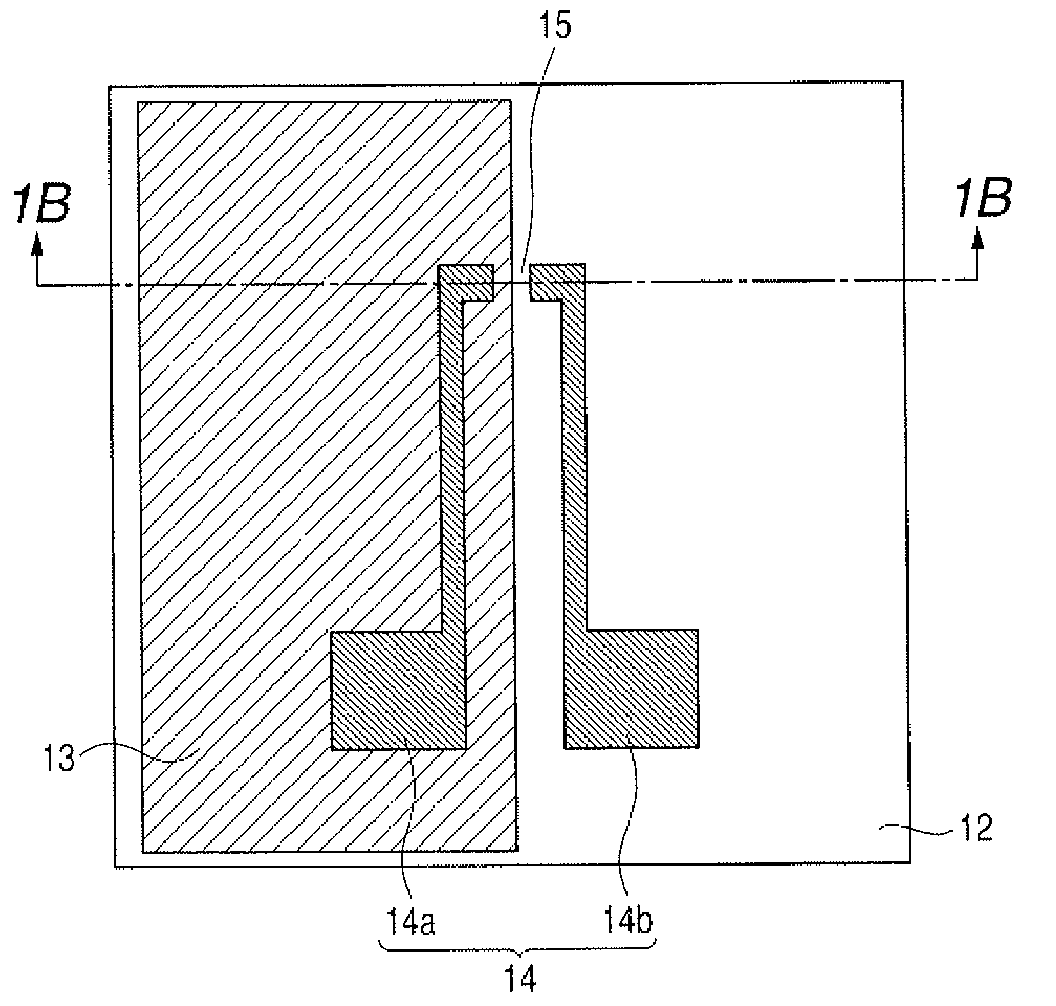
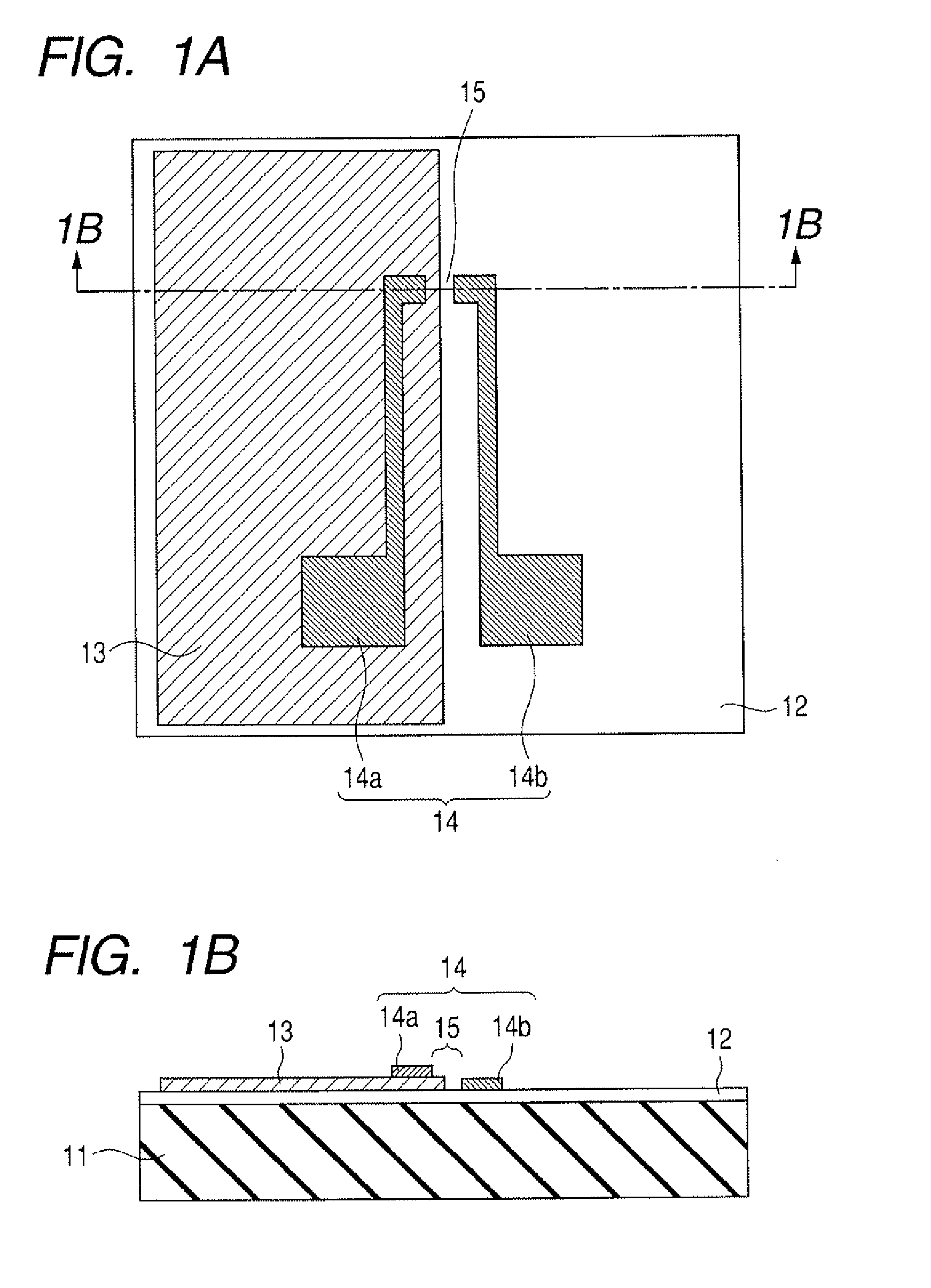
[0060]As shown in FIGS. 1A and 1B, in Example 1, a semi-insulating (SI-) InP substrate is used as the substrate 11. Further, an InGaAs thin film, formed on the SI-InP substrate 11 by epitaxial growth at about 250° C., is used as the photoconductive portion 12. Then, to adjust (increase) electric resistance, the InGaAs thin film 12 may be doped with Be in a concentration of about 1017 to about 1018 cm−3. The high resistance portion 13 is formed of a silicon nitride thin film or the like. The silicon nitride thin film 13 desirably has a thickness of less than 200 nm in order to obtain a moderate electric resistance. Moreover, the silicon nitride thin film 13 favorably has a higher resistance than the InGaAs thin film 12.

[0061]As shown in FIGS. 1A and 1B, the silicon nitride thin film 13 is formed so as to cover half of InGaAs thin film 12 by using plasma CVD, a photolithography, a dry etching method or the like. Subsequently, first and second conductive portions 14a, 14b formed by lam...

example 2

[0070]Example 2 of the present invention is described. In the present example, a mixture in which a small amount of metal particles are mixed in a dielectric is used as the high resistance portion in the terahertz wave generating device that has been described in Example 1.

[0071]Example 2 is described by using reference numerals given to the structure shown in FIGS. 3A and 3B. For example, MgF2 is deposited on the photoconductive portion 52 and subsequently gold is deposited thereon to about 10 nm. When the gold is about 5 nm to about 10 nm, a so-called island structure is formed rather than a uniform thin film. In island structures, striped gold clusters are formed in various places. Again, a series of the following steps are repeated: MgF2 is deposited again; and gold is deposited thereon to about 5 nm to about 10 nm. Such repetition results in the formation of network in MgF2 where gold clusters are connected. Therefore, an object having moderate electric conductivity is formed. ...

example 3

[0072]Example 3 of the present invention is described with reference to FIGS. 4C and 4D. A terahertz wave generating device which is a photoconductive device of the present example as shown in FIG. 4C and FIG. 4D which is a cross section view taken along line 4D-4D of FIG. 4C includes a substrate 91, a photoconductive portion 92, a high resistance portion 93, and first and second conductive portions 94a and 94b. The photoconductive portion 92 is provided in contact with at least a part of the upper surface of the substrate 91. The photoconductive portion 92 is not formed by a crystal growth on the substrate 91 but a thin film formed by a crystal growth on another substrate and attached onto the substrate 91. Thus, the photoconductive portion 92 employs a so-called thin-film transfer technology.

[0073]The material of the substrate 91 has a high transmittance for a terahertz wave. Such materials, for example, include high resistance silicon, quartz, polyethylene, polystyrene, fluorine-...


PUM


Abstract

A photoconductive device comprising a photoconductive portion for generating carriers by applied excitation light; a resistance portion in contact with the photoconductive portion; a first conductive portion in contact with the resistance portion; and a second conductive portion that is provided so as to have a gap with respect to the first conductive portion and is in contact with the photoconductive portion.

Description

BACKGROUND OF THE INVENTION[0001]1. Field of the Invention[0002]The present invention relates to a photoconductive device which can be used as an device for generating an electromagnetic wave in the frequency range of 30 GHz or more and 30 THz or less, i.e., in the frequency region from a so-called millimeter wave to a terahertz wave (which is also called a terahertz wave herein), and a method for producing the same, and apparatus using the same.[0003]2. Description of the Related Art[0004]In recent years, technological developments utilizing terahertz waves have become active. Japanese Patent Application Laid-Open No. 2002-223017 discusses a terahertz wave generating device. As shown in FIG. 10A and FIG. 10B which is a cross section view taken along line 10B-10B of FIG. 10A, the device includes a conductive portion 163 (163a and 163b) formed on a photoconductive portion 162 on a substrate 161 with the two sides separated from each other by a gap 165. One conductive portion 163a and...

Claims


Application Information

Patent Timeline
IPC IPC(8): H01L31/00
CPCH01L31/0352H01S1/02H01L31/09
Inventor KASAI, SHINTARO
Owner CANON KK
Why Eureka
Eureka Blog
Learn More