Gallium nitride epitaxial crystal, method for production thereof, and field effect transistor

a technology of gallium nitride and epitaxial crystal, which is applied in the direction of transistors, semiconductor devices, electrical devices, etc., can solve the problems of difficult to achieve high voltage resistance, device leads to breakdown, and low voltage resistance, so as to prevent the fluctuation of the threshold value of the transistor and the deterioration of the pinch-off characteristic, the effect of increasing the voltage resistance of the transistor

Active Publication Date: 2010-05-13
SUMITOMO CHEM CO LTD +1
View PDF2 Cites 9 Cited by
  • Summary
  • Abstract
  • Description
  • Claims
  • Application Information

AI Technical Summary

Benefits of technology

[0025]According to the present invention, the p-conductive type crystal layer for hole-withdrawing is counter-arranged on the lower layer of the source electrode in which holes accumulate and remain. This arrangement attempts to increase voltage resistance of a transistor. Additionally, an insulating layer is arranged at the lower part of the buffer layer lying from the gate electrode greatly affecting running characteristics of electrons to the drain electrode, and this arrangement can ef

Problems solved by technology

Actually, however, the high voltage resistance as expected is not achieved.
One of the reasons is a problem of hole-withdrawing.
As a result, positive feedback phenomenon occurs, and then, a device leads to breakdown later.
Even though band gap is large, it is not easy to achieve high voltage resistance commensurate with this.
According to the above conventional technology, a certain hole-withdrawing effect can be expected, but the technology has the following problems.
A p-conductive GaN type crystal layer is generally formed doping magnesium or the like in high concentration, and therefore it has poor crystalline quality.
As a result, an element active layer epitaxially grown on the crystal takes over poor crystalline quality of the p-conductive type

Method used


Image

  • Gallium nitride epitaxial crystal, method for production thereof, and field effect transistor
  • Gallium nitride epitaxial crystal, method for production thereof, and field effect transistor
  • Gallium nitride epitaxial crystal, method for production thereof, and field effect transistor

Examples


examples

[0072]The present invention is described in more detail by reference to the Examples, but the scope of the present invention is not limited to the Examples.

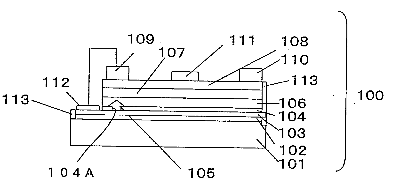
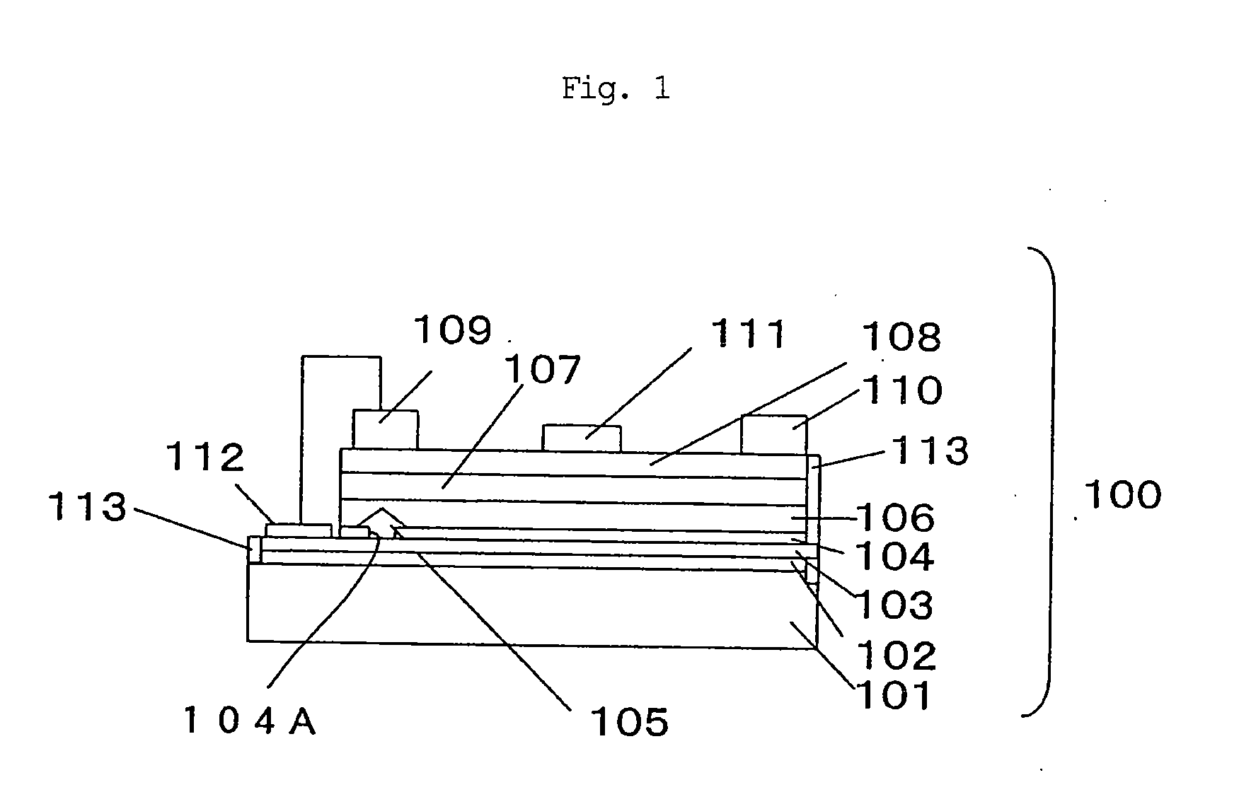
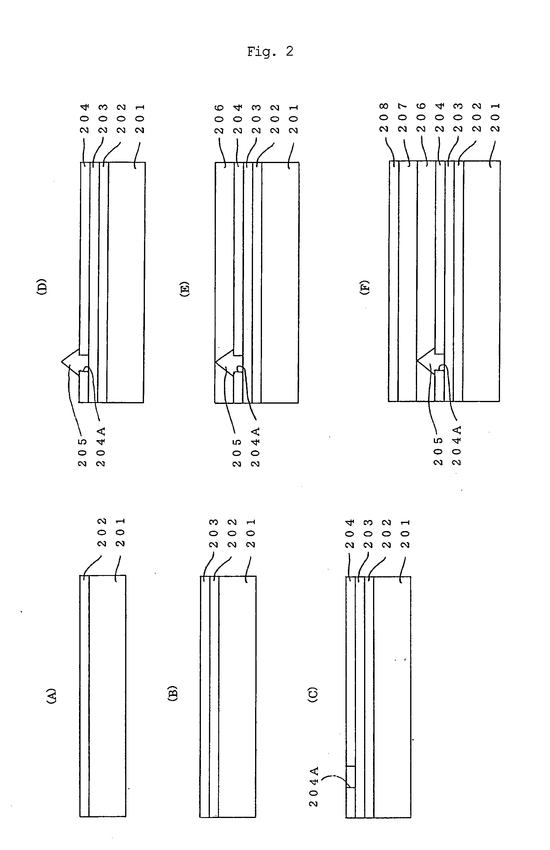
[0073]FIG. 2 shows production steps of a gallium nitride-based field effect transistor having the constitution shown in FIG. 1.

[Preparation of Gallium Nitride Type Epitaxial Crystal]

[0074]A silicon carbide base substrate 201 having growth surface of (0001) and an off-angle of 0.5° was set in a growing reactor. An aluminum nitride buffer layer 202 having a thickness of 2,000 nm was grown on the base substrate 201 by MOCVD method (FIG. 2(A)).

[0075]A p-conductive type gallium nitride crystal layer 203 having magnesium doped therein, having a thickness of 500 nm and Mg concentration of 5×1018 cm−2 was grown by changing a raw material gas and using a magnesium raw material as a dopant (FIG. 2(B)).

[0076]After cooling, the base substrate 201 was taken out of the reactor. The base substrate 201 was set to a CVD apparatus, and a silicon n...


PUM


Abstract

The present invention provides a gallium nitride type epitaxial crystal, a method for producing the crystal, and a field effect transistor using the crystal. The gallium nitride type epitaxial crystal comprises a base substrate and the following (a) to (e), wherein a connection layer comprising a gallium nitride type crystal is arranged in an opening of the non-gallium nitride type insulating layer to electrically connect the first buffer layer and the p-conductive type semiconductor crystal layer. (a) a gate layer, (b) a high purity first buffer layer containing a channel layer contacting an interface on the base substrate side of the gate layer, (c) a second buffer layer arranged on the base substrate side of the first buffer layer, (d) a non-gallium nitride type insulating layer arranged on the base substrate side of the second buffer layer, and having the opening at a part thereof, and (e) a p-conductive type semiconductor crystal layer arranged on the base substrate side of the insulating layer.

Description

TECHNICAL FIELD[0001]The present invention relates to a gallium nitride type (hereinafter referred to as a “GaN type”) epitaxial crystal for field effect transistor, a method for production thereof, and a field effect transistor using the crystal.BACKGROUND ART[0002]A gallium nitride based-field effect transistor is a device in which high voltage resistance is expected from a size of band gap of a material. Actually, however, the high voltage resistance as expected is not achieved. One of the reasons is a problem of hole-withdrawing. When high electric field is applied to a transistor to drive the transistor, running electrons collide with crystal lattices, and this collision causes the phenomenon of a so-called impact ionization in which electrons and holes are generated. Electrons generated by the phenomenon are rapidly absorbed in a drain electrode. However, holes merely move relatively slowly toward the lower part of a source electrode in the crystal layer, and as a result, the ...

Claims


Application Information

Patent Timeline
IPC IPC(8): H01L29/772H01L29/205H01L21/20
CPCH01L29/2003H01L29/7783H01L29/66462H01L29/1075H01L29/778H01L29/812H01L21/18
Inventor NISHIKAWA, NAOHIROSAZAWA, HIROYUKIHATA, MASAHIKO
Owner SUMITOMO CHEM CO LTD
Why Eureka
Try Eureka