Nanopatterned biopolymer optical device and method of manufacturing the same

a biopolymer and optical device technology, applied in the direction of instruments, other domestic objects, transportation and packaging, etc., can solve the problems of non-biodegradable materials, long time in the environment, and increased environmental pollution, so as to reduce environmental pollution, improve environmental protection, and improve environmental protection

Active Publication Date: 2010-05-13
TRUSTEES OF TUFTS COLLEGE TUFTS UNIV
View PDF6 Cites 121 Cited by
  • Summary
  • Abstract
  • Description
  • Claims
  • Application Information

AI Technical Summary

Benefits of technology

[0012]One advantage of the present invention is in providing optical devices that minimize the negative impact to the environment.
[0013]Another advantage of the present invention is in providing optical devices that are biocompatible.
[0014]Yet another advantage of the present invention is in providing optical devices that have additional functional features that are not provided by conventional optical devices.
[0015]In the above regard, inventors of the present invention recognized that biopolymers, and especially silk proteins, present novel structure and resulting functions. For example, from a materials science perspective, silks spun by spiders and silkworms represent the strongest and toughest natural fibers known and present various opportunities for functionalization, processing, and biocompatibility. Over five millennia of history accompany the journey of silk from a sought-after textile to a scientifically attractive fiber. As much as its features had captivated people in the past, silk commands considerable attention in this day and age because of its strength, elasticity, and biochemical properties. The novel material features of silks have recently been extended due to insights into self-assembly and the role of water in assembly. These insights, in turn, have led to new processing methods to generate hydrogels, ultrathin films, thick films, conformal coatings, three-dimensional porous matrices, solid blocks, nanoscale diameter fibers, and large diameter fibers.
[0016]Silk-based materials achieve their impressive mechanical properties with natural physical crosslinks of thermodynamically stable protein secondary structures also known as beta sheets (β-sheets). Thus, no exogenous crosslinking reactions or post-processing crosslinking is required to stabilize the materials. The presence of diverse amino acid side chain chemistries on silk protein chains facilitates coupling chemistry to functionalize silks, such as with cytokines, morphogens, and cell binding domains. There are no known synthetic or biologically-derived polymer systems that offer this range of material properties or biological interfaces, when considering mechanical profiles, aqueous processing, ease of functionalization, diverse modes of processing, self-forming crosslinks, biocompatibility, and biodegradability.
[0017]While no other biopolymer or synthetic polymer can match the range of features outlined above for silk, the inventors of the present invention have identified some other polymers that exhibit various properties similar or analogous to silk. In particular, other natural biopolymers including chitosan, collagen, gelatin, agarose, chitin, polyhydroxyalkanoates, pullan, starch (amylose amylopectin), cellulose, hyaluronic acid, and related biopolymers, or a combination thereof, have been identified. In view of the above noted features of biopolymers and of silk in particular, the present invention provides various novel nanopatterned biopolymer optical devices and methods for manufacturing such devices.

Problems solved by technology

However, these optical devices, and the fabrication methods employed in their manufacture, generally involve significant use of non-biodegradable materials.
Such materials are not biodegradable and remain in the environment for extended periods of time after the optical devices are removed from service and discarded.
However, recycling also requires expenditures of natural resources, and adds to the environmental costs associated with such materials.
Therefore, there exists an unfulfilled need for optical devices that minimize the negative impact to the environment.
In addition, there exists an unfulfilled need for optical devices that provide additional functional features that are not provided by conventional optical devices.

Method used


Image

  • Nanopatterned biopolymer optical device and method of manufacturing the same
  • Nanopatterned biopolymer optical device and method of manufacturing the same
  • Nanopatterned biopolymer optical device and method of manufacturing the same

Examples


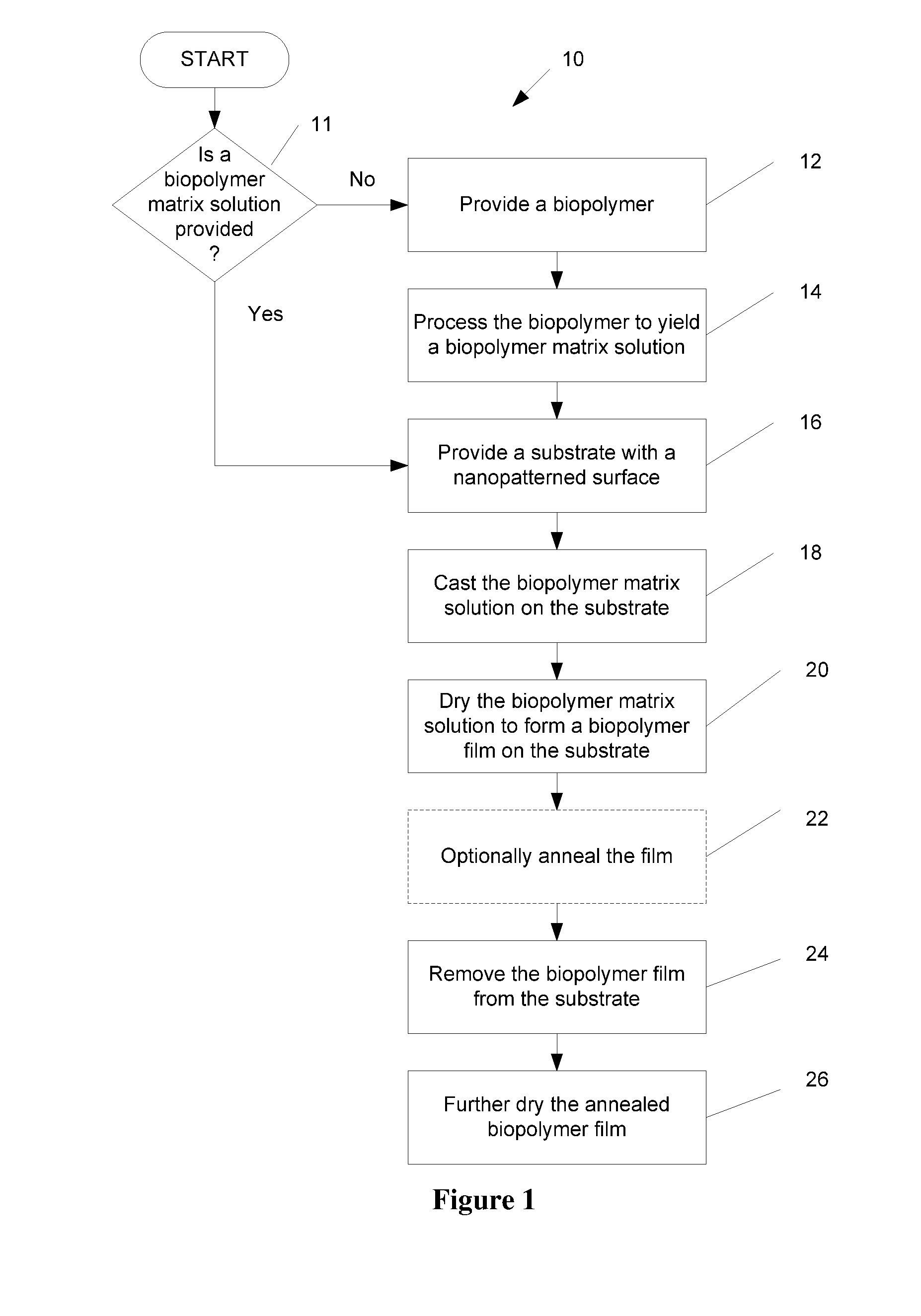
Embodiment Construction

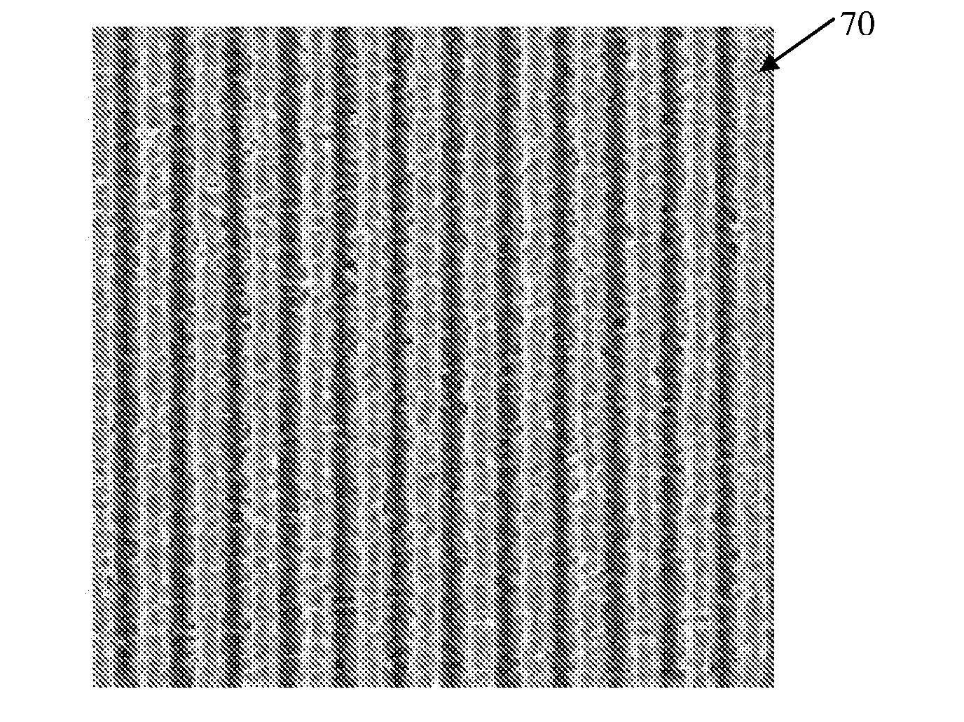
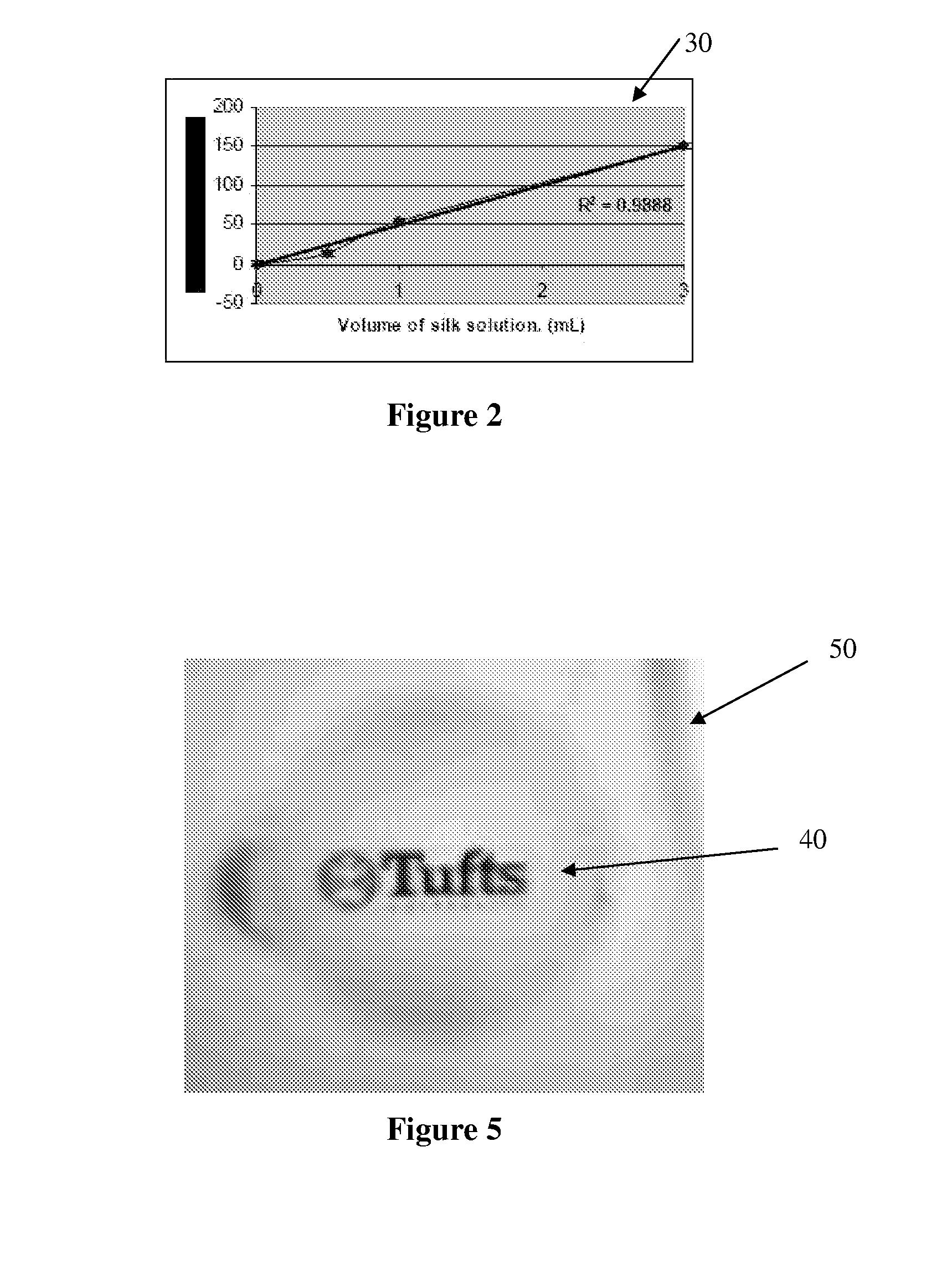
[0055]As described in detail below, the nanopatterned biopolymer optical devices in accordance with the present invention have been fabricated using a biopolymer such as silk. In this regard, the silk utilized was silkworm silk. However, there are many different silks, including spider silk, transgenic silks, and genetically engineered silks, variants and combinations thereof and others, that may alternatively be used in accordance with the present invention to obtain a nanopatterned biopolymer optical device.

[0056]In addition, other biodegradable polymers may be used instead of silk. For example, additional biopolymers, such as chitosan, exhibit desirable mechanical properties, can be processed in water, and form generally clear films for optical applications. Other biopolymers, such as chitosan, collagen, gelatin, agarose, chitin, polyhydroxyalkanoates, pullan, starch (amylose amylopectin), cellulose, hyaluronic acid, and related biopolymers, or a combination thereof, may alternat...


PUM

PropertyMeasurementUnit
wt %aaaaaaaaaa
sizesaaaaaaaaaa
sizesaaaaaaaaaa

Abstract

A method of manufacturing a nanopatterned biopolymer optical device includes providing a biopolymer, processing the biopolymer to yield a biopolymer matrix solution, providing a substrate with a nanopatterned surface, casting the biopolymer matrix solution on the nanopatterned surface of the substrate, and drying the biopolymer matrix solution to form a solidified biopolymer film on the substrate, where the solidified biopolymer film is formed with a surface having a nanopattern thereon. In another embodiment, the method also includes annealing the solidified biopolymer film. A nanopatterned biopolymer optical device includes a solidified biopolymer film with a surface having a nanopattern is also provided.

Description

CROSS-REFERENCE TO RELATED APPLICATIONS[0001]This application claims the benefit of priority of U.S. Provisional Application Ser. No. 60 / 856,297 filed on Nov. 3, 2006, entitled “Biopolymer Devices and Methods for Manufacturing the Same.” This application also claims the benefit of priority of U.S. Provisional Application Ser. No. 60 / 907,502, filed on Apr. 5, 2007, entitled “Nanopatterned Biopolymer Optical Device and Method of Manufacturing the Same.”GOVERNMENT SUPPORT[0002]The invention was made with government support under grant number FA95500410363 awarded by the Air Force Office of Scientific Research. The government has certain rights in this invention.BACKGROUND OF THE INVENTION[0003]1. Field of the Invention[0004]The present invention is directed to nanopatterned biopolymer optical devices, and methods for manufacturing such devices.[0005]2. Description of Related Art[0006]The field of optics is well established. Some subfields of optics include diffractive optics, micro-opt...

Claims


Application Information

Patent Timeline
Patent Type & Authority Applications(United States)
IPC IPC(8): B29D11/00G02B1/12G02B1/04C12N11/08
CPCB29D11/00G02B1/04Y10T428/24479C08L1/00C08L3/00C08L5/00C08L89/00
Inventor KAPLAN, DAVID L.OMENETTO, FIORENZOLAWRENCE, BRIANCRONIN-GOLOMB, MARKGEORGAKOUDI, IRENE
Owner TRUSTEES OF TUFTS COLLEGE TUFTS UNIV
Why Eureka
Try Eureka