RF transceiver IC having internal loopback conductor for ip2 self test

a transceiver and internal loopback technology, applied in the direction of transmission monitoring, line-fault/interference reduction, semiconductor/solid-state device details, etc., can solve the problem that the factory calibration cannot account for performance changes that occur due, the input impedance of linear amplifiers is generally only small, and the performance change is generally small. , to achieve the effect of maximizing power transfer, reducing power consumption, and low input impedan

Active Publication Date: 2010-05-13
QUALCOMM INC
View PDF13 Cites 65 Cited by
  • Summary
  • Abstract
  • Description
  • Claims
  • Application Information

AI Technical Summary

Benefits of technology

[0011]In a first novel aspect, the transmit mixer of the transmit chain of the RF transceiver integrated circuit is a current mode output mixer. The receive mixer of the receive chain of the RF transceiver integrated circuit is a passive mixer that has a relatively low input impedance. Rather than using an active mixer in the receive chain, a passive mixer is used that is followed by a transimpedance amplifier (TIA). The TIA outputs a voltage proportional to its input current received from the passive mixer. In the loopback mode, the transmit mixer drives a two tone current signal to the passive mixer via the segmented loopback conductor. Other portions of the transceiver are controlled to maximize power transfer from the transmit chain to the receive chain during the loopback mode, and to reduce power consumption, and to prevent unwanted RF transmissions from occurring. In a normal operating mode of the RF transceiver integrated circuit, the...

Problems solved by technology

A linear amplifier generally introduces only a small amount of second order distortion when the amplifier is operating at a low output power level.
Although such factory calibration may allow the cellular telephone transceiver to be calibrated to account for variations in the semiconductor fabrication process used to make transceiver integrated circuits, such factory calibration cannot account for performance changes that occur due to temperature changes that occur during operation of the cellular telephone.
Similarly, such factory calibration cannot account for performance changes that occur due to voltage supply variations that occur during operation of the cellular telephone transceiver.
First, an unnecessarily large amount of power that even may exceed a maximum output power rating of the transceiver can be driven back onto the transceiver's antenna during calibration. Usually the power level of the blocker used in calibration testing is higher than the power level of the blocker specified in standards to detect a nonlinear effect.
Second, the one tone blocker approach utilizes an...

Method used


Image

  • RF transceiver IC having internal loopback conductor for ip2 self test
  • RF transceiver IC having internal loopback conductor for ip2 self test
  • RF transceiver IC having internal loopback conductor for ip2 self test

Examples


Embodiment Construction

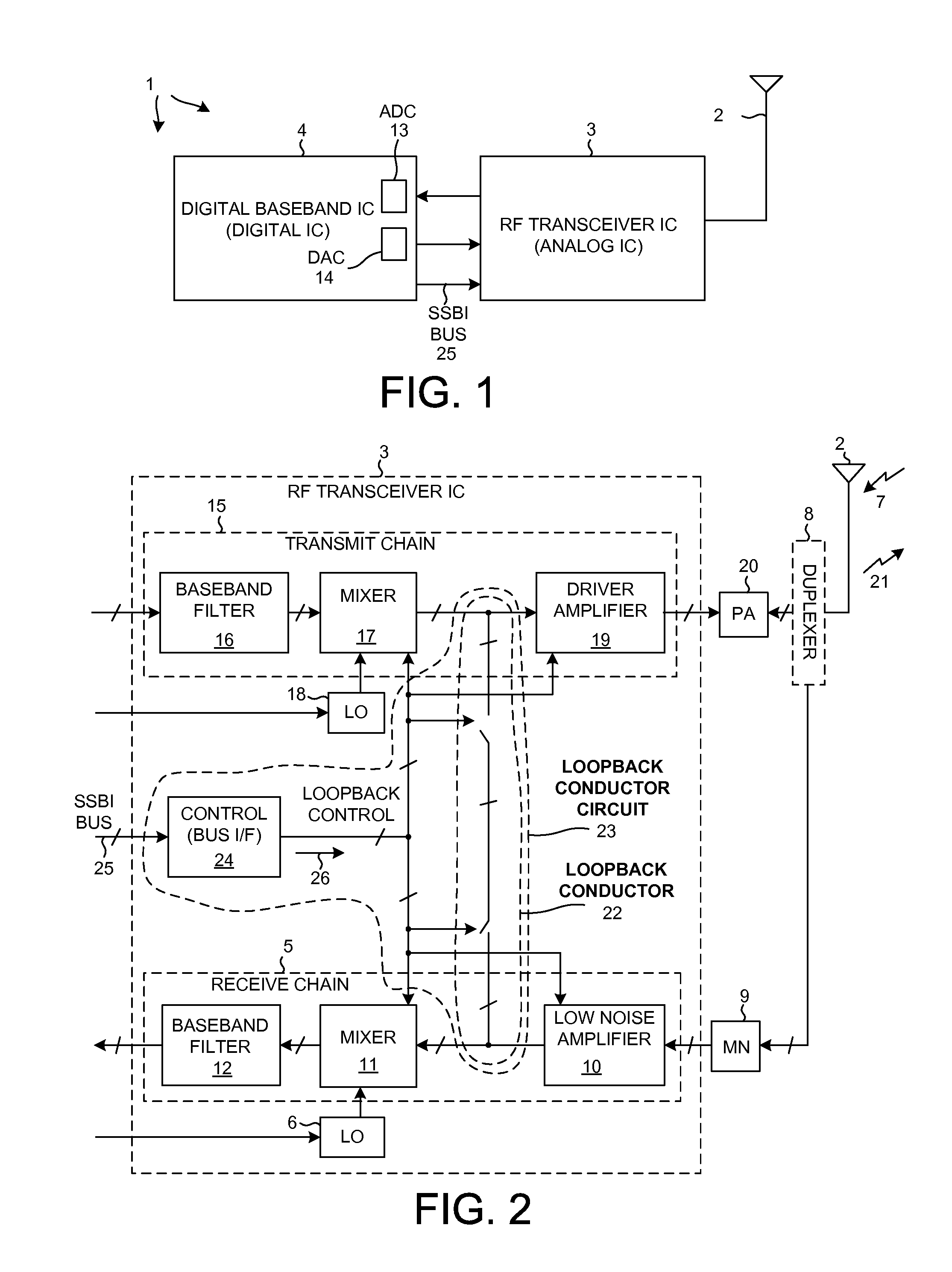
[0023]FIG. 1 is a very simplified high level block diagram of one particular type of mobile communication device 1 in accordance with one novel aspect. In this particular example, mobile communication device 1 is a cellular telephone that uses a Code Division Multiple Access (CDMA) or an Orthogonal Frequency Division Multiple Access (OFDMA) cellular telephone communication protocol. The cellular telephone includes (among several other parts not illustrated) an antenna 2 and two integrated circuits 3 and 4. Integrated circuit 4 is called a “digital baseband integrated circuit” or a “baseband processor integrated circuit”. Integrated circuit 3 is an RF transceiver integrated circuit. RF transceiver integrated circuit 3 is called a “transceiver” because it includes a transmitter as well as a receiver.

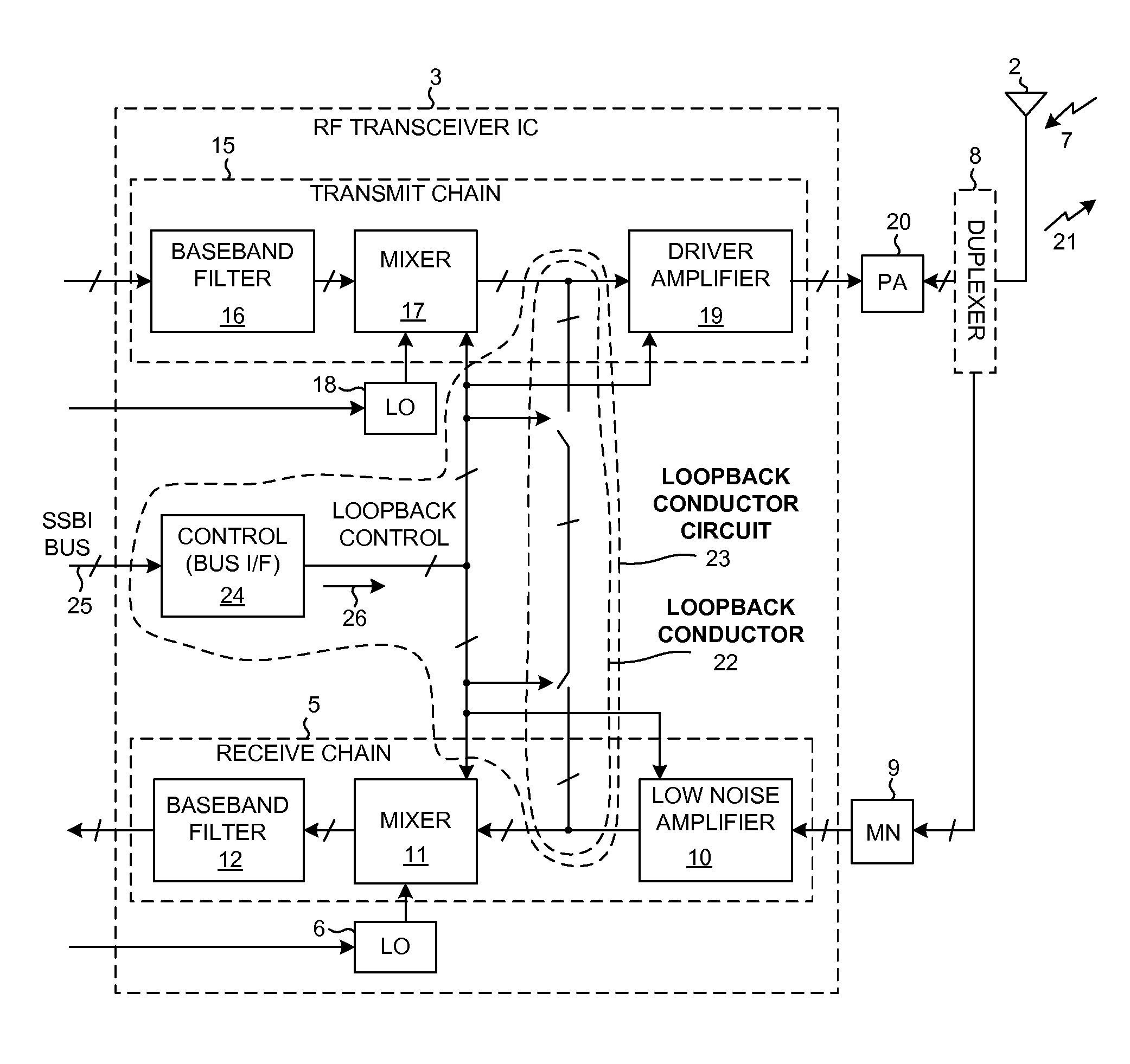
[0024]FIG. 2 is a more detailed block diagram of the RF transceiver integrated circuit 3. The receiver includes what is called a “receive chain”5 as well as a local oscillator (LO) 6. When...


PUM


Abstract

An RF transceiver integrated circuit has a novel segmented, low parasitic capacitance, internal loopback conductor usable for conducting IP2 self testing and/or calibration. In a first novel aspect, the transmit mixer of the transceiver is a current mode output mixer. The receive mixer is a passive mixer that has a low input impedance. In the loopback mode, the transmit mixer drives a two tone current signal to the passive mixer via the loopback conductor. In a second novel aspect, only one quadrature branch of the transmit mixer is used to generate both tones required for carrying out an IP2 test. In a third novel aspect, a first calibration test is performed using one quadrature branch of the transmit mixer at the same time that a second calibration test is performed using the other quadrature branch, thereby reducing loopback test time and power consumption.

Description

BACKGROUND INFORMATION[0001]1. Technical Field[0002]The disclosed embodiments relate to internal loopback testing and calibration of RF transceivers.[0003]2. Background Information[0004]Both the transmitter and the receiver of a cellular telephone are ideally linear devices that introduce minimal distortion into the signal being communicated. One type of distortion is referred to as second-order distortion. A linear amplifier generally introduces only a small amount of second order distortion when the amplifier is operating at a low output power level. As the output power increases, however, the output power at the fundamental frequency (the frequency of the input signal) rises at a first rate with respect to overall rising output power, whereas the output power due to second-order distortion rises at a faster rate. When the output power of the amplifier is high enough, the output power of the second-order distortion reaches the output power of the fundamental signal. This point of ...

Claims


Application Information

Patent Timeline
IPC IPC(8): H04B17/00
CPCH04B1/40H03D7/168H04B1/48H04B17/00H03D7/00
Inventor KO, JIN-SUKOHLMANN, MICHAELAHRARI, BAHMAN
Owner QUALCOMM INC
Why Eureka
Try Eureka