Wafer support jig, vertical heat treatment boat including wafer support jig, and method for manufacturing wafer support jig
- Summary
- Abstract
- Description
- Claims
- Application Information
AI Technical Summary
Benefits of technology
Problems solved by technology
Method used
Image
Examples
example 1
Samples A to E
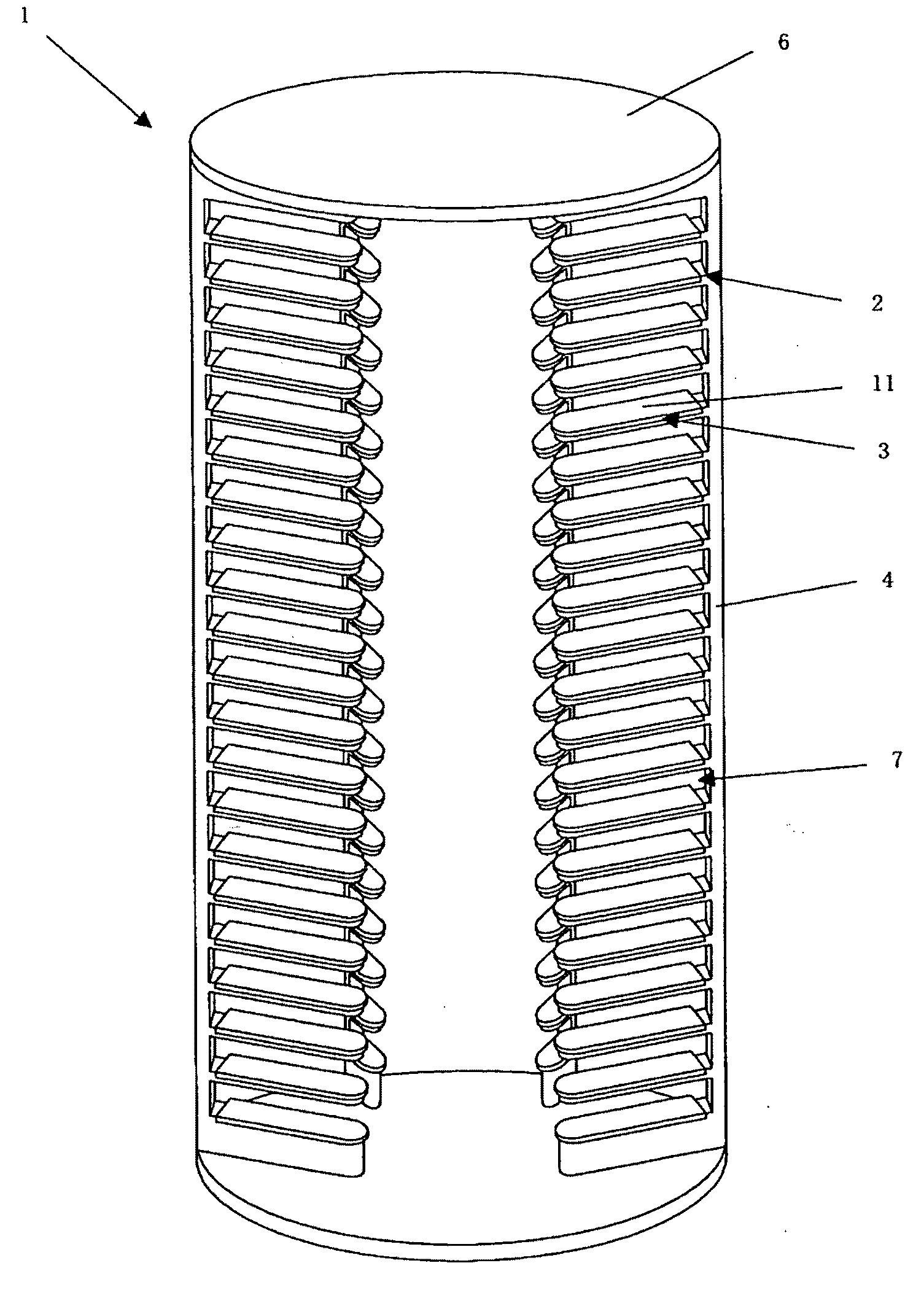
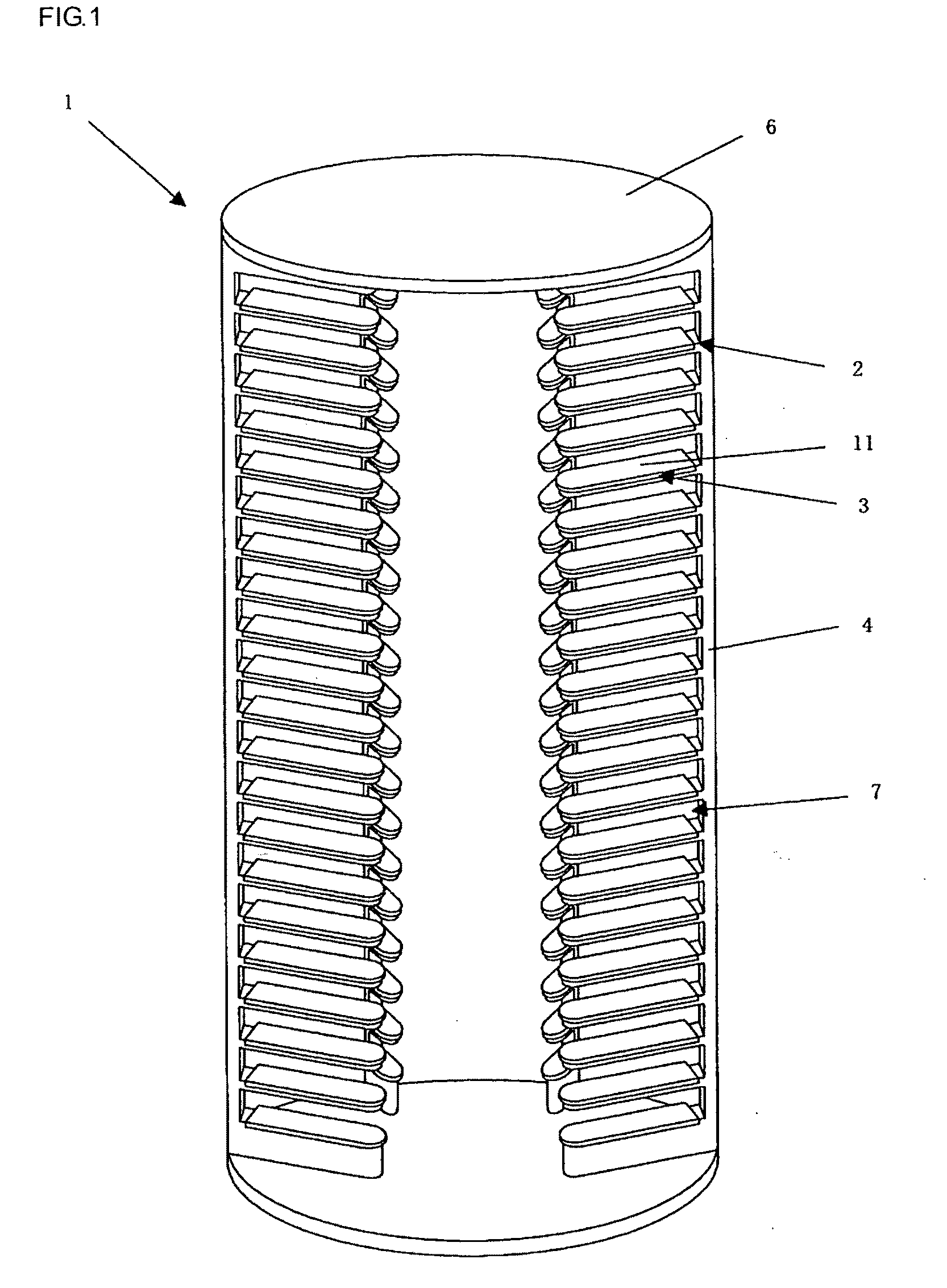
[0116]A material obtained by mixing silicon carbide powder in a slurry having silica-glass powder / water / methyl cellulose mixed therein was injected into a die to be molded, then demolded, dried, degreased, purified, sintered, and ground, thereby fabricating such a wafer support jig (a length: 30 mm) as shown in FIG. 1.
[0117]As the silicon carbide powder, powder having the greatest frequency size of 8 μm, the maximum size of 24 μm or below, and the minimum size of 3 μm or above in a size frequency distribution was used, and five types of materials having different mixing ratios were prepared.
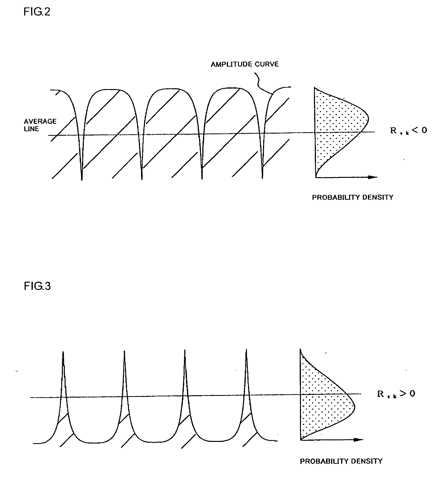
[0118]After grinding, etching was carried out by using 10% HF for four hours to expose silicon carbide particles on a surface, thus fabricating wafer support jigs having different Rsk values.
[0119]Table 1 shows a result of measuring a value Ra, a value Rsk, and a density of the protruding objects on each wafer support jig by using Form Talysurf Intra. Further, a protruding object ha...
example 2
[0140]In the same wafer support jig as that fabricated in Comparative Example 3, the five protruding objects having the heights of 30 μm or above were all ground down.
[0141]Slip dislocation was evaluated like Example 1, and slip dislocation was no longer detected.
example 3
[0142]A wafer support jig made of polycrystal silicon was fabricated by grinding.
[0143]At this time, there was no protrusion having a height of 2 μm or above, Ra was 0.16 μm and Rsk was −0.10.
[0144]When this wafer support jig was annealed in an argon gas atmosphere at a reduced pressure and 1250° C. for 100 hours, Ra was 0.24 μm, Rsk was 0.95, and a density of protruding objects each having a height of 2 μm or above and less than 30 μm was 1.5×10³ pieces / mm2 within arbitrary 1 mm2. Further, there was no protruding object having a height of 30 μm or above on the entire support surface, namely, the wafer support jig according to the present invention was obtained.
[0145]When this wafer support jig was used to perform the same heat treatment as that in Example 1, slip dislocation was not detected in the X-ray topography evaluation.
PUM
| Property | Measurement | Unit |
|---|---|---|
| Length | aaaaa | aaaaa |
| Length | aaaaa | aaaaa |
| Area | aaaaa | aaaaa |
Abstract
Description
Claims
Application Information


