Semiconductor nanowire and its manufacturing method

Active Publication Date: 2010-06-03
JOLED INC
View PDF8 Cites 37 Cited by
  • Summary
  • Abstract
  • Description
  • Claims
  • Application Information

AI Technical Summary

Benefits of technology

[0035]According to the method of the present invention, a process step that can be carried out easily is added, thus making it possible to control the shape of the nanowire being formed at a nanometer scale in the growth axis direction.
[0036]In addition, if the nanowire fabricated by the method of the present invention is used, there is no need to perform a process step for controlling the structure (such as ion implantation) or its accompanying

Problems solved by technology

However, according to the conventional photolithography technology, the feature size cannot be reduced unlimitedly.
Al

Method used


Image

  • Semiconductor nanowire and its manufacturing method
  • Semiconductor nanowire and its manufacturing method
  • Semiconductor nanowire and its manufacturing method

Examples


embodiment 1

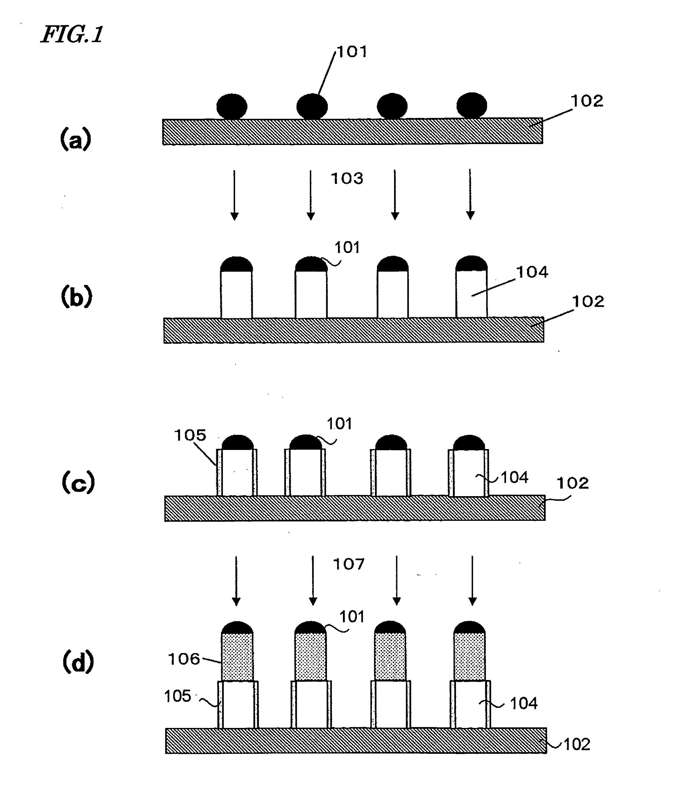
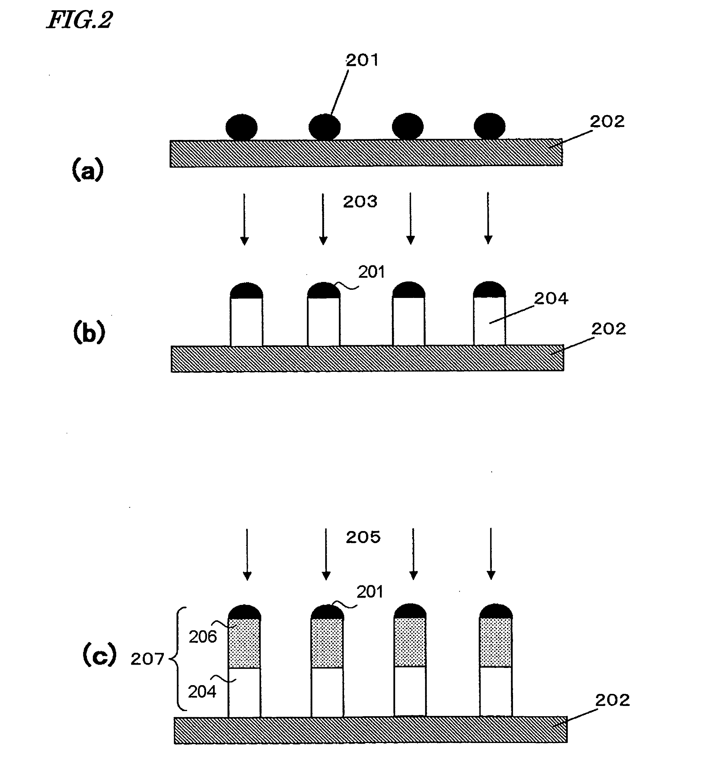
[0067]A first specific preferred embodiment of a semiconductor nanowire manufacturing process according to the present invention will be described with reference to FIGS. 2(a) through 3(c). In this preferred embodiment, Si nanowires that have been doped to have a p-i-p structure are formed.

[0068]First, as shown in FIG. 2(a), a silicon substrate 202 is provided as a growth substrate and catalyst particles 201 of gold (Au) are put on the silicon substrate 202. The silicon substrate 202 just needs to have thermal resistance that is high enough to withstand the heat treatment temperature on the nanowires growing. That is why a silicon dioxide film or a silicon nitride film may have been deposited on the silicon substrate 202. The crystallographic plane orientation and resistivity of the silicon substrate 202 may be determined arbitrarily.

[0069]The Au particles 201 used as the catalyst particles have distinct ability to promote the decomposition of the source gas and are used to produce ...

embodiment 2

[0094]Hereinafter, a second preferred embodiment of a method for fabricating a semiconductor nanowire according to the present invention will be described with reference to FIGS. 11(a) through 11(d). In this preferred embodiment, nanowires with a heterostructure of GaAs and GaAsP (which will be referred to herein as “GaAs / GaAsP nanowires”) are formed. These nanowires can be grown by VLS growth mechanism, which is a known method.

[0095]First, as shown in FIG. 11(a), Au particles 301 are put on an arbitrary substrate 302 by the method described above, for example.

[0096]Next, the substrate 302 with these Au particles 301 is loaded into the chamber of a CVD system, for example. Then, as shown in FIG. 11(b), a source gas 303, including a constituent element of GaAs nanowires, is introduced into the chamber and maintained at a predetermined pressure. And the substrate 302 is heated by a lamp or a heater, for example, and maintained at an arbitrary temperature, thereby growing GaAs nanowire...

embodiment 3

[0102]Hereinafter, a semiconductor device will be described as a third specific preferred embodiment of the present invention. The semiconductor device of this preferred embodiment is a transistor including the Si nanowires of the first preferred embodiment (which will be referred to herein as “profile Si nanowires”).

[0103]FIG. 12 is a perspective view illustrating a transistor including the profile Si nanowires (which will be referred to herein as a “nanowire transistor”) as a third preferred embodiment of the present invention. FIG. 13(a) is a top view of the nanowire transistor shown in FIG. 12 and FIG. 13(b) is a cross-sectional view as viewed on the plane C-C shown in FIG. 13(a).

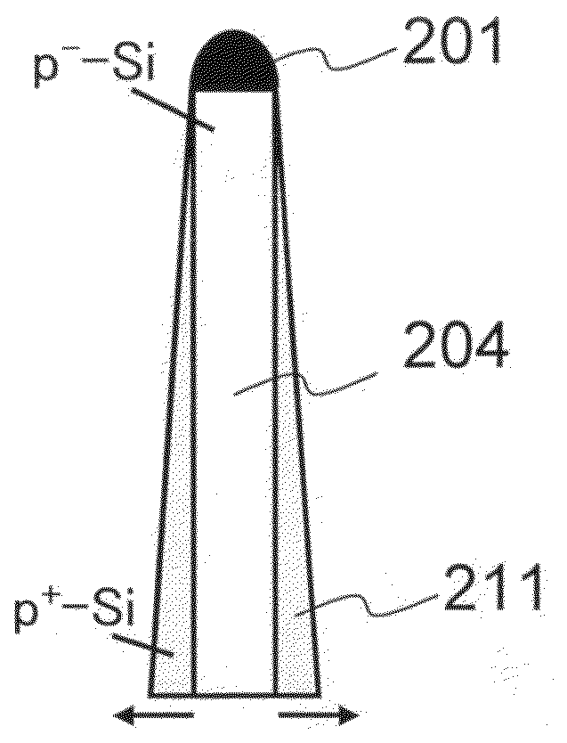
[0104]In each of the profile Si nanowires 406 of this preferred embodiment, the p-type doped regions 407 are doped with a Group III element such as B at a dose of approximately 1×10¹⁸ atoms / cm3 to approximately 1×10²⁰ atoms / cm3, while the non-doped region 408 includes a Group III element such as B in a ...


PUM


Abstract

A method for fabricating a semiconductor nanowire that has first and second regions is provided. A catalyst particle is put on a substrate. A first source gas is introduced, thereby growing the first region from the catalyst particle via a vapor-liquid-solid phase growth. A protective coating is formed on a sidewall of the first region, and a second source gas is introduced to grow the second region extending from the first region via the liquid-solid-phase growth.

Description

TECHNICAL FIELD[0001]The present invention relates to a semiconductor nanowire and a method for fabricating the same.BACKGROUND ART[0002]Researches and developments have been carried on extensively in order to reduce the feature sizes of transistors for large-scale integrated circuits (LSIs) or thin-film transistors (TFTs) for flat-panel displays. In a silicon semiconductor process, fine line patterning with a design rule of 0.1 μm or less is realized by shortening the wavelength of an exposing radiation source for use in a photolithographic process. However, according to the conventional photolithography technology, the feature size cannot be reduced unlimitedly. Also, as the feature size has been reduced, the costs of exposure systems and masking members have been rising steeply.[0003]Meanwhile, carbon nanotubes (see Non-Patent Document No. 1) and nanowires made of a material with semiconductor type properties (see Patent Document No. 1) have attracted a lot of attention recently....

Claims


Application Information

Patent Timeline
IPC IPC(8): H01L29/775H01L21/04
CPCB82Y10/00Y10S438/962C30B11/12C30B25/00C30B29/06C30B29/40C30B29/60H01L21/02521H01L21/02573H01L21/02603H01L21/02653H01L21/02656H01L27/3262H01L29/0665H01L29/0673H01L29/0676H01L29/068H01L29/775H01L33/18B82Y30/00H10K59/1213
Inventor KAWASHIMA, TAKAHIROSAITOH, TOHRU
Owner JOLED INC
Why Eureka
Try Eureka