Method and apparatus for backside illuminated image sensors using capacitively coupled readout integrated circuits

a capacitive coupled readout and image sensor technology, applied in the field of semiconductor-based image sensors, can solve the problems of long exposure time, high cost and complexity of silicon ccd fabrication process, and the limitation of conventional image sensors to silicon charge coupled devices (ccds), etc., to achieve high scanning rate, increase the dynamic range of pixel, and high dynamic range

Inactive Publication Date: 2010-06-10
TELEDYNE SCI & IMAGING
View PDF12 Cites 146 Cited by
  • Summary
  • Abstract
  • Description
  • Claims
  • Application Information

AI Technical Summary

Benefits of technology

[0018]In another embodiment, an image sensor implemented in two physical layers each implemented in separate chips. First layer contains array of pixels that contains photodiodes and mostly analog front-end pixel circuits as well as necessary readout circuit modules outside the pixel array to read out the analog pixel value. To overcome the saturation problem of the typical CMOS sensors, integrator is reset multiple times during exposure, and this has been communicated to the second layer to keep track of the count of reset operations. Therefore, first layer only contains the analog integrator value since the las

Problems solved by technology

Conventional image sensors were limited to silicon charge coupled devices (CCDs).
The fabrication process for silicon CCDs has always been expensive and complex.
For dim objects, a long exposure time is required to collect sufficiently large number of photons.
There is also a limit on the maximum exposure time due to the inherent dark current of the pixel.
However, increased circuit complexity requires larger pixels to fit all the required analog and digital circuit bloc

Method used


Image

  • Method and apparatus for backside illuminated image sensors using capacitively coupled readout integrated circuits
  • Method and apparatus for backside illuminated image sensors using capacitively coupled readout integrated circuits
  • Method and apparatus for backside illuminated image sensors using capacitively coupled readout integrated circuits

Examples


Embodiment Construction

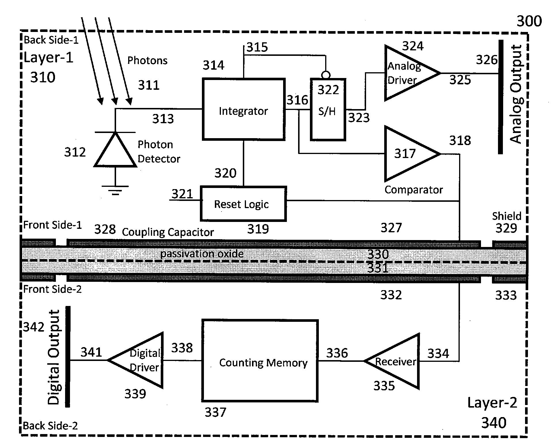
[0024]FIG. 3 shows a circuit block diagram 300 according to an embodiment of the present invention. The functional embodiment of FIG. 3 can be implemented at pixel level in linear or plane array format using two physical layers, layer-1310 and layer-2340. In one embodiment, each pixel of an array of pixels independently implements the embodiment of FIG. 3. In FIG. 3, photons 311 are received by photon detector 312. Photon detector 312 can comprise any conventional photosensitive element such as a photodiode.

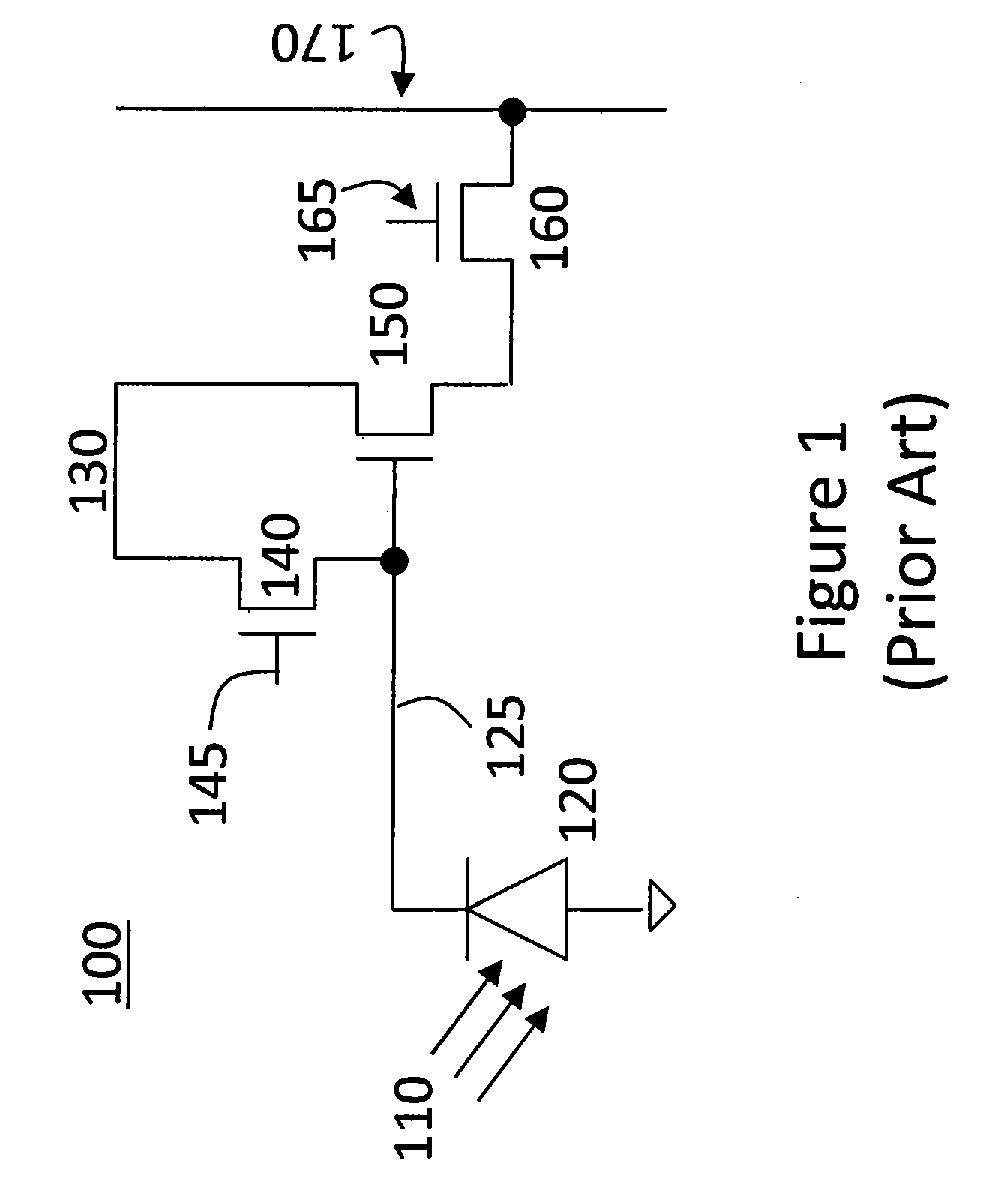
[0025]Photon detector 312 can be readout in different ways using the conventional three transistor (3-T) pixel structure shown in FIG. 1 or using more advanced pixel readout circuits using a capacitive trans-impedance amplifier (CTIA), which is basically an integrator. The CTIA has the advantage of providing constant detector reverse bias potential during exposure. Charge signal 313, generated by photon detector 312, is accumulated by integrator 314. In the case of the 3-T pixel,...


PUM


Abstract

The images sensor includes a readout circuit capacitatively coupled to a memory circuit. The readout circuit includes: (i) a photon detector to receive a plurality of photons and to provide a charge signal corresponding to the received photons, (ii) a resettable integrator that is reset multiple times over a single exposure time and provides an analog representation of the incident photons during the last integration cycle, and (iii) a comparator that monitors the integrator output and generates a reset pulse when the integrator reaches a built-in threshold value. The memory circuit includes: (i) a receiver circuit that detects the output of the digital driver in the front-end readout circuit via capacitive coupling and generates a digital voltage pulse for each received signal, and (ii) a digital counting memory to count the received pulses to provide a coarse digital representation of how many times the integrator is reset.

Description

BACKGROUND[0001]1. Field[0002]The disclosure relates to semiconductor based image sensors and more particularly to backside illuminated Active Pixel image Sensors (APS) with advanced pixel level signal processing capabilities using capacitively coupled readout integrated circuits (ROICs).[0003]2. Related Art[0004]Conventional APS are defined by solid state imaging devices having an array of pixels arranged in columns and rows. Each pixel contains both a photo sensing means and at least one other active component which create a charge that is converted to a voltage or a current signal. The converted signal indicates the amount of light incident upon a pixel. Conventional image sensors were limited to silicon charge coupled devices (CCDs). Over the years, CCDs have become the standard for visible image sensors. The fabrication process for silicon CCDs has always been expensive and complex. As a result, considerable attention has been paid to developing complementary metal-oxide (CMOS)...

Claims


Application Information

Patent Timeline
IPC IPC(8): H01L27/00
CPCH01L27/14634H01L27/1469H04N5/3745H01L27/1464H04N5/378H04N5/35536H04N5/37455H01L2224/16145H04N25/58H04N25/772H04N25/79H04N25/77H04N25/75
Inventor EMINOGLU, SELIMLAUXTERMANN, STEFAN C.
Owner TELEDYNE SCI & IMAGING
Why Eureka
Try Eureka