

Dielectric ceramics, and laminated ceramic capacitor
a technology of laminated ceramic and dielectric ceramic, which is applied in the direction of ceramics, fixed capacitor electrodes, fixed capacitors, etc., can solve the problems of deterioration in reliability, increase the possibility of occurrence of defective articles, and decrease in dielectric, so as to improve the ac voltage characteristics of capacitance, improve the ac voltage characteristics, and improve the effect of ac voltage characteristics
- Summary
- Abstract
- Description
- Claims
- Application Information
AI Technical Summary
Benefits of technology
Problems solved by technology
Method used
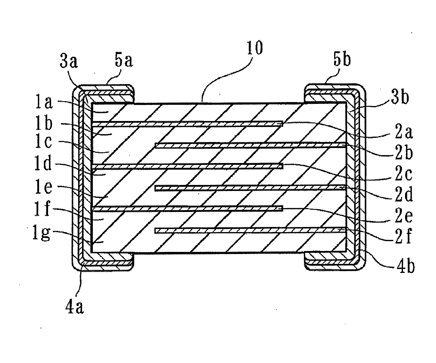
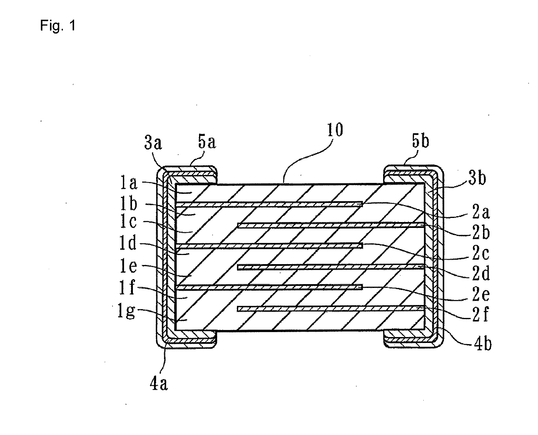
Image

Examples
example 1
Preparation of Sample
Sample No. 1
[0086]As ceramic base materials, BaCO3, TiO2, and NiO were prepared, and these ceramic base materials were weighed so that the blending ratio m between Ba and Ti was 1.010, and the molar part a of NiO relative to 100 parts by mol of BaTiO3 was 1.0.
[0087]Next, these weighed materials were put into a ball mill together with PSZ balls and pure water, wet mixed and ground for 48 hours, and calcined at a temperature of 1100° C. to prepare a calcined powder.
[0088]Next, as additive materials, Dy2O3, MnCO3, MgCO3, and SiO2 were prepared. Then these additive materials were weighed so that the dielectric ceramic satisfied the following general formula (B).
100Ba1.010TiO3+aNiO+1.0DyO3 / 2+0.3MnO+1.0MgO+1.5SiO2
[0089]These additive materials were put into a ball mill together with the calcined powder, wet mixed in the ball mill for 24 hours, and then dried by evaporation to obtain a ceramic material powder.
[0090]Then, to the ceramic material powder was added a poly...
example 2
Preparation of Sample
Samples Nos. 11 to 18
[0118]A ceramic material powder having the same composition as that in Sample No. 1 was prepared and a ceramic laminate was obtained.
[0119]Next, the ceramic laminate was subjected to a binder removing treatment at a temperature of 300° C., and each sample was subjected to a burning treatment which was conducted for about two hours under a reductive atmosphere of H2—N2—H2O gas whose oxygen partial pressure was controlled to 10−9 to 10−12 MPa at different temperatures ranging from 1140 to 1220° C. to obtain laminated ceramic capacitors of Sample Nos. 11 to 18.
Sample Nos. 19 to 26
[0120]Laminated ceramic capacitors of Sample Nos. 19 to 26 burnt at different temperatures were obtained in a similar manner and procedure as that in Sample Nos. 11 to 18 except that NiO was not added.
Structural Analysis of Ceramic Texture
[0121]For each sample of Sample Nos. 11 to 26, the structure of a ceramic texture was analyzed in a manner similar to Example 1, and...
example 3
Preparation of Sample
[0132]As ceramic base materials, BaCO3, TiO2, and NiO were prepared, and these ceramic base materials were weighed so that the blending molar ratio m between Ba and Ti and the molar part a of NiO relative to 100 parts by mol of BaTiO3 were the values as shown in Table 5, and a calcined powder was prepared in a similar manner and procedure as in Example 1.
[0133]Next, as additive materials, R oxides containing a rare earth element R (La2O3, CeO2, Pr6O11, Nd2O3, Sm2O3, Eu2O3, Gd2O3, Tb2O3, Dy2O3, Ho2O3, Er2O3, Tm2O3, Yb2O3, Lu2O3, Y2O3), M oxides containing a metal element M (MnO, Fe2O3, CuO, CoO, V2O5, WO3, Cr2O3, MoO2, Al2O3), MgO, and SiO2 were prepared.
[0134]Then these additive materials were weighed so that b, c, d and e in the following general formula (C) of the dielectric ceramic satisfied the values shown in Table 5.
100BamTiO3+aNiO+bROn+cMOv+dMgO+eSiO2
[0135]Next, these additive materials were mixed with the calcined powder in a ball mill, and then dried b...
PUM
| Property | Measurement | Unit |
|---|---|---|
| AC voltage | aaaaa | aaaaa |
| dielectric constant | aaaaa | aaaaa |
| dielectric constant | aaaaa | aaaaa |
Abstract
Description
Claims
Application Information