Scatterometry metrology target design optimization

a technology of scattering metrology and target design optimization, applied in the field of semiconductor/solid-state device testing/measurement, instruments, photomechanical equipment, etc., can solve the problems of slow and costly trial and error based design, inability to widely spread the rules themselves, and time-consuming approach, so as to reduce the cycle time and improve the peak target performance

Active Publication Date: 2010-07-08
KLA TENCOR TECH CORP
View PDF30 Cites 67 Cited by
  • Summary
  • Abstract
  • Description
  • Claims
  • Application Information

AI Technical Summary

Benefits of technology

[0045]Embodiments of the present invention can reduce the cycle time to reach an optimal metrology tar

Problems solved by technology

Unfortunately, in a trial and error approach each trial represents a new reticle and a set of experiments with the new reticle to test the performance of the target.
This is often a time consuming approach.
Consequently, trial and error based design tends to be slow and costly.
In addition “rules of thumb” are often considered intellectual property

Method used


Image

  • Scatterometry metrology target design optimization
  • Scatterometry metrology target design optimization
  • Scatterometry metrology target design optimization

Examples


Embodiment Construction

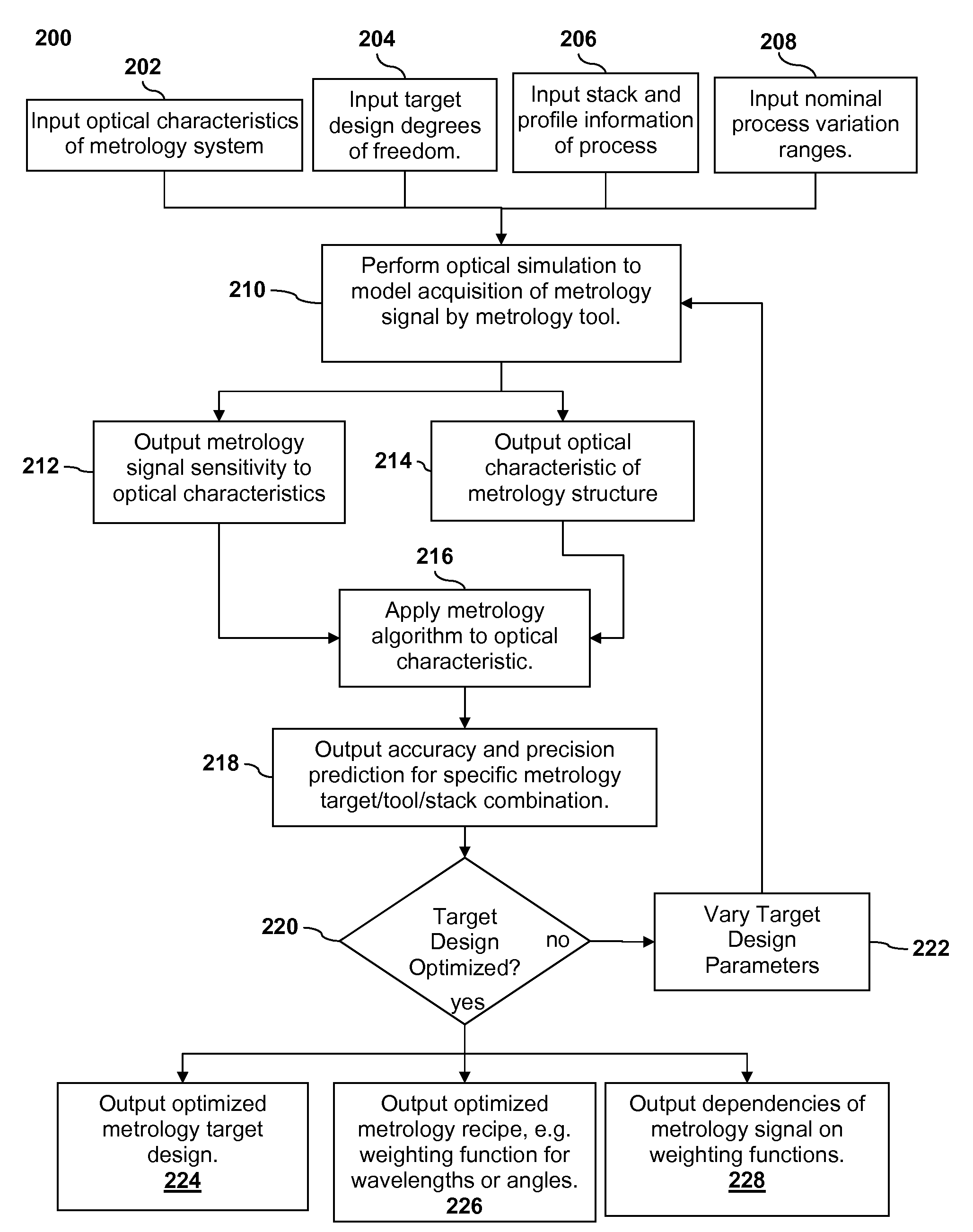
[0013]Although the following detailed description contains many specific details for the purposes of illustration, anyone of ordinary skill in the art will appreciate that many variations and alterations to the following details are within the scope of the invention. Accordingly, the exemplary embodiments of the invention described below are set forth without any loss of generality to, and without imposing limitations upon, the claimed invention.

[0014]According to an embodiment of the present invention a piece of software (or two or more pieces of interacting software) may be used to optimize a metrology target structure that can be output in a standard format. By way of example, and not by way of limitation, the standard format may be GDS II stream format, commonly referred to by the acronym GDSII, which is a database file format that is an industry standard for data exchange of integrated circuit or IC layout artwork. GDSII is a binary file format representing planar geometric sha...


PUM


Abstract

A metrology target design may be optimized using inputs including metrology target design information, substrate information, process information, and metrology system information. Acquisition of a metrology signal with a metrology system may be modeled using the inputs to generate one or more optical characteristics of the metrology target. A metrology algorithm may be applied to the characteristics to determine a predicted accuracy and precision of measurements of the metrology target made by the metrology system. Part of the information relating to the metrology target design may be modified and the signal modeling and metrology algorithm may be repeated to optimize the accuracy and precision of the one or more measurements. The metrology target design may be displayed or stored after the accuracy and precision are optimized.

Description

FIELD OF THE INVENTION[0001]This invention generally relates to semiconductor fabrication and more particularly to the use of interferometry in measuring the shape and thickness variation of a semiconductor substrate.BACKGROUND OF THE INVENTION[0002]As the components of semiconductor devices shrink to smaller and smaller sizes, now on the order of nanometers, the ability to improve metrology performance, productivity, and device correlation becomes ever so important. To determine the alignment of features formed in one layer with respect to features formed in a previous or subsequent layer, metrology targets are often formed in one or more of the layers. The metrology targets facilitate measurement of the dimensions of features and alignment, e.g., overlay, between the features using a metrology tool such as a critical dimension (CD) scanning electron microscope (SEM) or scatterometer. In the past, metrology target optimization was performed experimentally by trial and error, and by...

Claims


Application Information

Patent Timeline
IPC IPC(8): G06F17/50
CPCG03F7/705H01L22/12G03F7/70683G03F7/70633H01L21/0273G03F7/706839G03F7/706831
Inventor ADEL, MICHAELMANASSEN, AMNONKANDEL, DANIEL
Owner KLA TENCOR TECH CORP
Why Eureka
Try Eureka