Semiconductor device and method of manufacturing the same

a technology of semiconductors and semiconductors, applied in the direction of semiconductor devices, electrical devices, transistors, etc., can solve the problems of difficult control of work functions, inability to solve the above-described problems, and inability to control work functions, so as to prevent the effect of fermi level pinning and reduce the amount of change in work functions

Inactive Publication Date: 2010-08-05
RENESAS ELECTRONICS CORP
View PDF7 Cites 19 Cited by
  • Summary
  • Abstract
  • Description
  • Claims
  • Application Information

AI Technical Summary

Benefits of technology

[0043]In the present invention, the barrier film, which contains Si, O and C as major constituents, or contains Si, N and C as major constituents, is provided between the Hf-containing insulating film and the fully-silicided gate electrode. The barrier film blocks diffusion of at least Hf which composes the insulating film and a metal element which composes the fully-silicided gate electrode. Accordingly, also the diffusion of Hf metal may be suppressed, and thereby Fermi level pinning is prevented from occurring. In addition, since the diffusion of the metal element may be suppressed, and since the dielectric constant of the barrier film is smaller than that of the silicon oxynitride film, so that the fully-silicided gate electrode may be prevented from being elevated in the dielectric constant at the interface. Accordingly, the effect of controlling the work function inducible by the segregated impurity may fully be expressed, without reducing the amount of change in work function.

Problems solved by technology

According to the description, the high-k film may be exposed on the side faces thereof to plasma in the process of forming the gate electrode, and may be damaged due to electric charge injected therethrough.
It has, however, been difficult to control the work function, even with the above-described method of avoiding Fermi level pinning.
For this reason, the segregated impurity is supposed to fail in fully exhibiting an effect of modifying the work function, and thereby the control of work function is supposed to made more difficult as described in the above.
These films are, however, incapable of solving the above-described problem for the reason described below.
Aluminum oxide, aluminum nitride and aluminum oxynitride, which contain Al as an constitutive element, have large dielectric constants, and are therefore apparently make the control of work function more difficult due to elevated dielectric constants at the interface of the impurity-segregated FUSI electrode.
Also silicon oxide and silicon oxynitride are poor in the barrier performance against Hf diffusion, and allows inclusion of Hf as a consequence, and again less expectable in keeping the dielectric constant at a low level.
Silicon carbide having no oxygen cannot suppress reaction with the silicidation metal, but is silicided by itself, and is not expectable for keeping the dielectric constant at a low level.
As a consequence, the control of work function still remains in difficulty, even if the barrier films described in International Patent Publication WO 2004 / 073072 Pamphlet are used.
Since the amount of carbon introduced by the method disclosed in the Publication falls short of the amount enough to be accountable as a major constituent of the “carbonized layer”, so that it is considered difficult for such carbonized layer to suppress diffusion of major constituents such as Hf or the silicide-composing metal.
In conclusion, the control of work function still remains in difficulty, even if the carbonized layer described in the Publication is adopted.

Method used


Image

  • Semiconductor device and method of manufacturing the same
  • Semiconductor device and method of manufacturing the same
  • Semiconductor device and method of manufacturing the same

Examples


first embodiment

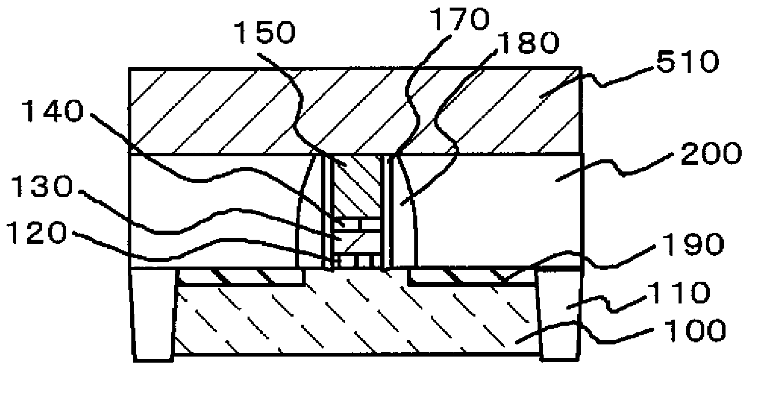
[0050]Aiming at solving the above-described problems, the present inventors have extensively been investigated into a stacked structure of a Hf-containing, high-k gate insulating film and a fully-silicided gate electrode in a semiconductor device, and a method of manufacturing the same. In particular, keeping difficulty in the control of work function inducible by the segregate impurity in our mind, the present inventors have been making special efforts on removing the difficulty in such stacked structure. Preferred embodiments of the present invention will be explained below, referring to the attached drawings. Note that any similar constituents in all drawings will be given similar reference numerals or symbols, and explanations therefor will not be repeated.

[0051]What is brought into our focus was characteristics of the barrier film, and more specifically a balance between the dielectric constant and barrier performance against diffusion of metal.

[0052]As descried in the above, t...

second embodiment

[0102]A second embodiment of the present invention relates to replacement of the NMIS transistor in the first embodiment with a PMIS. A method of manufacturing the PMIS transistor of this embodiment is similar to that described in the first embodiment, except for aspects of difference described below. The aspects of difference relate to that the ion implantation into the channel is carried out using an N-type impurity, that the impurity to be doped into the polysilicon electrode is B, as one example of P-type impurities, and that the conductivity type of the impurities to be implanted into the extension region, the pocket region, and the source / drain regions are inverted.

[0103]The PMIS transistor of this embodiment having the NiSi fully-silicided electrode and the gate insulating film, obtained as described the above, was found to have a work function of the gate electrode of 4.9 eV, as judged from the C—V characteristics. It was also found that the work function of the PMIS transis...

third embodiment

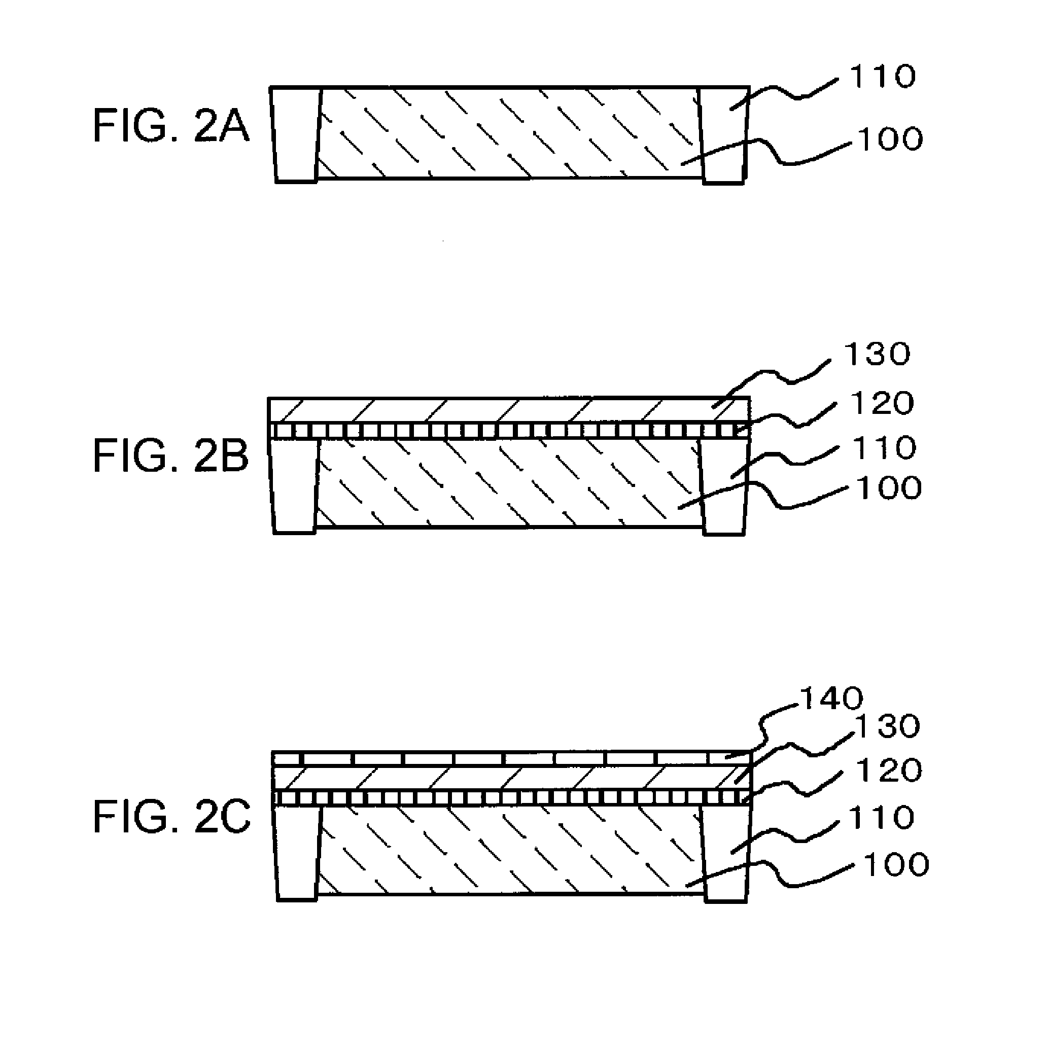
[0107]A third embodiment of the present invention is different from the above-described first and second embodiments, in that the substrate is not heated in the process of forming the barrier film, but instead annealed in an oxidation atmosphere gas, after the SiC target was sputtered in reactive sputtering in a non-oxidation atmosphere gas. Any other processes in the third embodiment are same as those in the first and second embodiments, as illustrated in FIG. 2A to FIG. 5B.

[0108]Aspects of the third embodiment, different from those in the first and second embodiments, will be explained below referring to FIGS. 6A and 6B.

[0109]After completion of the process illustrated in FIG. 2B, the SiC target was sputtered in an Ar atmosphere by DC sputtering, to thereby form a SiC film 340 of 0.3 nm thick on the HfSiON film 130 (FIG. 6A). The substrate herein was not heated. The compositional ratio of carbon in the finally obtainable SiOC film was found to be approximately 15 atm %, which was ...


PUM


Abstract

Provided is a semiconductor device of the present invention including, a substrate; a Hf-containing insulating film (HfSiON film) provided over the semiconductor substrate; a NiSi fully-silicided electrode for blocking diffusion of at least Hf which composes the insulating film and a metal element which composes the fully-silicided gate electrode, provided over the HfSiON film; and a barrier film (SiOC film) provided between HfSiON film and the NiSi fully-silicided electrode so as to be brought into contact with the NiSi fully-silicided electrode, wherein the NiSi fully-silicided electrode contains either an N-type or a P-type impurity segregated in a portion thereof brought into contact with the SiOC film, and the SiOC film has a dielectric constant not larger than that of a silicon oxynitride film, and contains (i) silicon (Si), (ii) carbon (C), and (iii) oxygen (O) or nitrogen (N), as major constituents.

Description

[0001]This application is based on Japanese patent application No. 2009-024068 the content of which is incorporated hereinto by reference.BACKGROUND[0002]1. Technical Field[0003]The present invention relates to a semiconductor device a method of manufacturing the same.[0004]2. Related Art[0005]International Patent Publication WO 2004 / 073072 describes a method of manufacturing a MIS semiconductor device. The method of manufacturing a semiconductor device is aimed at preventing growth of a low-k layer (silicon oxide film) between a substrate and a high-k film in a MOSFET which uses the high-k film as a gate insulating film, according to which a high-k film and a diffusion barrier layer are deposited on the substrate, the high-k film is annealed to modify film properties, a gate electrode material film is then deposited, and the films are then patterned to form a gate electrode. According to the description, the high-k film may be exposed on the side faces thereof to plasma in the proc...

Claims


Application Information

Patent Timeline
Patent Type & Authority Applications(United States)
IPC IPC(8): H01L29/78H01L21/28
CPCH01L21/28097H01L21/28123H01L21/28185H01L21/28202H01L29/4975H01L29/7833H01L29/517H01L29/518H01L29/66507H01L29/6659H01L29/513
Inventor HASE, TAKASHI
Owner RENESAS ELECTRONICS CORP
Why Eureka
Try Eureka