Methods and Apparatuses for Manufacturing Cast Silicon From Seed Crystals

Inactive Publication Date: 2010-08-05
AMG IDEAL CAST SOLAR +1
View PDF84 Cites 32 Cited by
  • Summary
  • Abstract
  • Description
  • Claims
  • Application Information

AI Technical Summary

Benefits of technology

[0019]In accordance with the present invention, there is also provided a crucible for the casting of silicon having a bottom surface and a plurality of side walls, wherein at least one of the plurality of side walls tapers inwards toward a center of the crucible at an angle from about 1° to about 25° with respect to a plane perpendicular to a bottom surface of the crucible and viewed in a direction extending upwards from the bottom surface. The tapered side wall or walls may reduce the vessel cross-sectional area taken in the direction away from the bottom surfac

Problems solved by technology

Imperfections can include individual impurities, agglomerates of impurities, intrinsic lattice defects and structural defects in the silicon lattice, such as dislocations and stacking faults.
Many of t

Method used


Image

  • Methods and Apparatuses for Manufacturing Cast Silicon From Seed Crystals
  • Methods and Apparatuses for Manufacturing Cast Silicon From Seed Crystals
  • Methods and Apparatuses for Manufacturing Cast Silicon From Seed Crystals

Examples


example 1

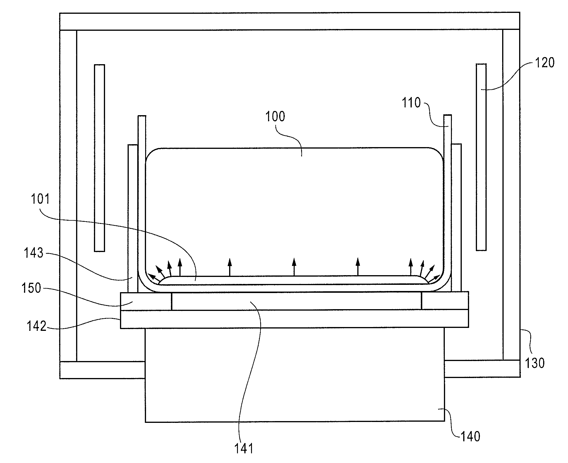
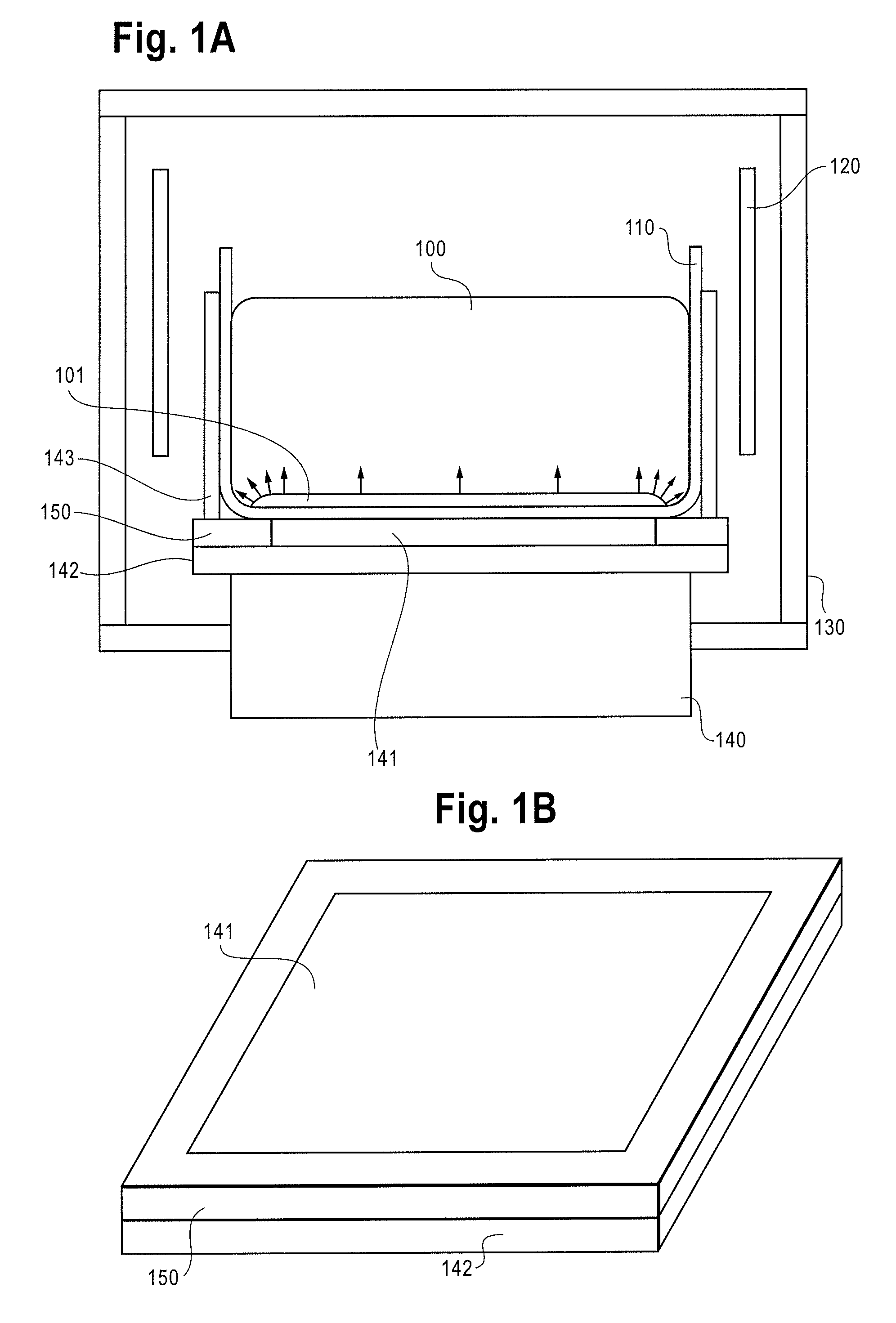
[0089]Crucible preparation: A crucible was placed on a supporting structure consisting of two layers. The bottom layer of the supporting structure is a solid isomolded graphite plate measuring 80 cm by 80 cm by 2.5 cm which supported a composite layer. The upper composite layer had an inner region that was a thermally conducting isomolded graphite plate measuring 60 cm by 60 cm by 1.2 cm, and was surrounded on all sides by a 10 cm perimeter of thermally insulating graphite fiber board of 1.2 cm thickness. In this way, the composite layer completely covered the bottom layer.

[0090]Seed preparation: A boule of pure Czochralski (CZ) silicon (monocrystalline) obtained from MEMC, Inc. and having 0.3 ppma of boron, was cut down along its length using a diamond coated band saw so that it had a square cross section measuring from 140 mm per side. The resulting block of monocrystalline silicon was cut through its cross section using the same saw into slabs having a thickness of about 2 cm to ...

example 2

[0092]Seeding was accomplished as in Example 1, and an ingot was cast containing a large monocrystalline volume. After cooling, the ingot was stood on its side and loaded into a band saw with fixed diamond abrasive for cutting. The bottom of the ingot was cut off as a single layer with a thickness of 2 cm. This layer was then fixed horizontally on a cutting table. In the same band saw, the edges of the layer were trimmed such that approximately 1.5 cm was removed from each side. The slab was then sandblasted to remove glue and foreign materials, after which it was etched in a hot sodium hydroxide bath, rinsed, and dipped in a HCl bath to remove metals. The slab was then placed on the bottom of a standard crucible of the same size as the previous ingot. Silicon feedstock was loaded to a total mass of 265 kg and the casting process was repeated, producing a second seeded ingot.

example 3

[0093]Seed preparation: A seed layer was prepared, starting with 18 kg of square, (100), plates used to line the bottom of a crucible, providing a coverage area of 58 by 58 cm and a thickness ranging from 2-3 cm. These plates were placed together into a larger square that was centered in the crucible. Next, this square was surrounded by a 2 cm thick layer of (111) oriented seed crystals, making the total seed layer a 63 cm by 63 cm square.

[0094]Casting: The crucible containing the seeds was filled with silicon to a total mass of 265 kg and placed in a casting station. Casting was performed as in Example 1, monitoring the process to assure that the seed layer remained intact through the end of melt and beginning of solidification. The resulting ingot was cut into a 5×5 grid of 12.5 cm bricks. Optical inspection of the crystal structure of the bricks showed that the (111) crystals acted as a buffer layer, preventing the ingress of randomly nucleated grains into the (100) volume.


PUM

PropertyMeasurementUnit
Lengthaaaaaaaaaa
Fractionaaaaaaaaaa
Fractionaaaaaaaaaa

Abstract

Methods and apparatuses are provided for casting silicon for photovoltaic cells and other applications. With these methods, an ingot can be grown that is low in carbon and whose crystal growth is controlled to increase the cross-sectional area of seeded material during casting.

Description

[0001]This application claims the benefit of U.S. Provisional Application No. 60 / 951,155, filed Jul. 20, 2007. The entire disclosure of U.S. Provisional Application No. 60 / 951,155 is hereby incorporated by reference into this specification.[0002]This application was made with U.S. Government support under Subcontract No.: ZAZ-6-33628-11 under prime contract with the National Renewable Energy Laboratory awarded by the Department of Energy. The Government has certain rights in this invention.DESCRIPTION[0003]1. Technical Field[0004]The present invention generally relates to the field of photovoltaics and to methods and apparatuses for manufacturing cast silicon for photovoltaic applications. The invention further relates to new forms of cast silicon that can be used to manufacture devices, such as photovoltaic cells and other semiconductor devices. The new silicon can have a monocrystalline, near-monocrystalline, bi-crystal, or geometric multicrystalline structure and can be manufactu...

Claims


Application Information

Patent Timeline
IPC IPC(8): H01L31/18B29C39/14B28B1/54B29C35/16
CPCC30B11/003C30B29/06F27B14/06H01L31/1804H01L31/182Y02E10/546Y10T428/12528C30B11/02C30B19/067H01L31/0312H01L31/036Y10T117/1092Y02E10/547Y02P70/50
Inventor STODDARD, NATHAN G.WU, BEICLARK, ROGER F.CLIBER, JAMES A.
Owner AMG IDEAL CAST SOLAR
Why Eureka
Try Eureka