

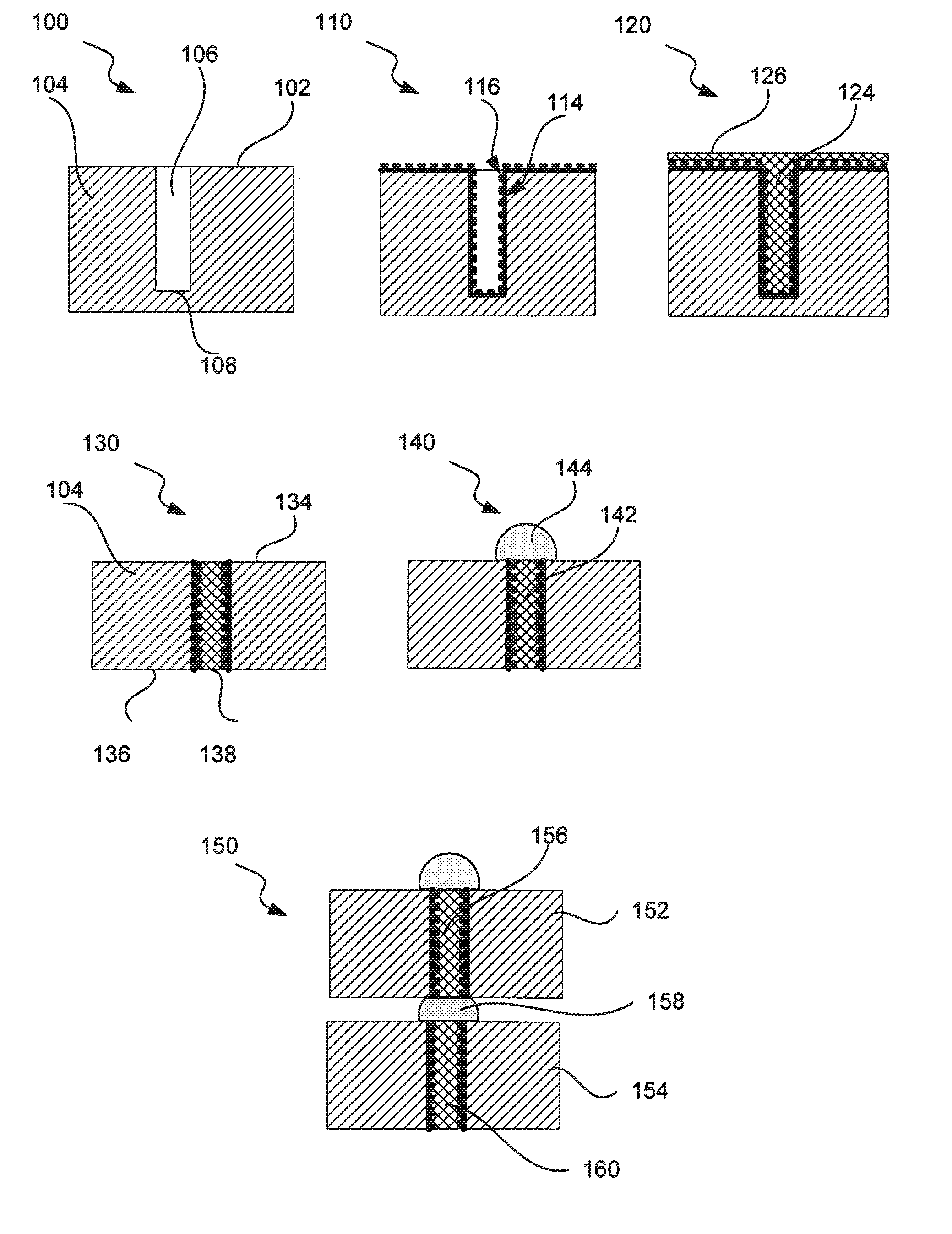
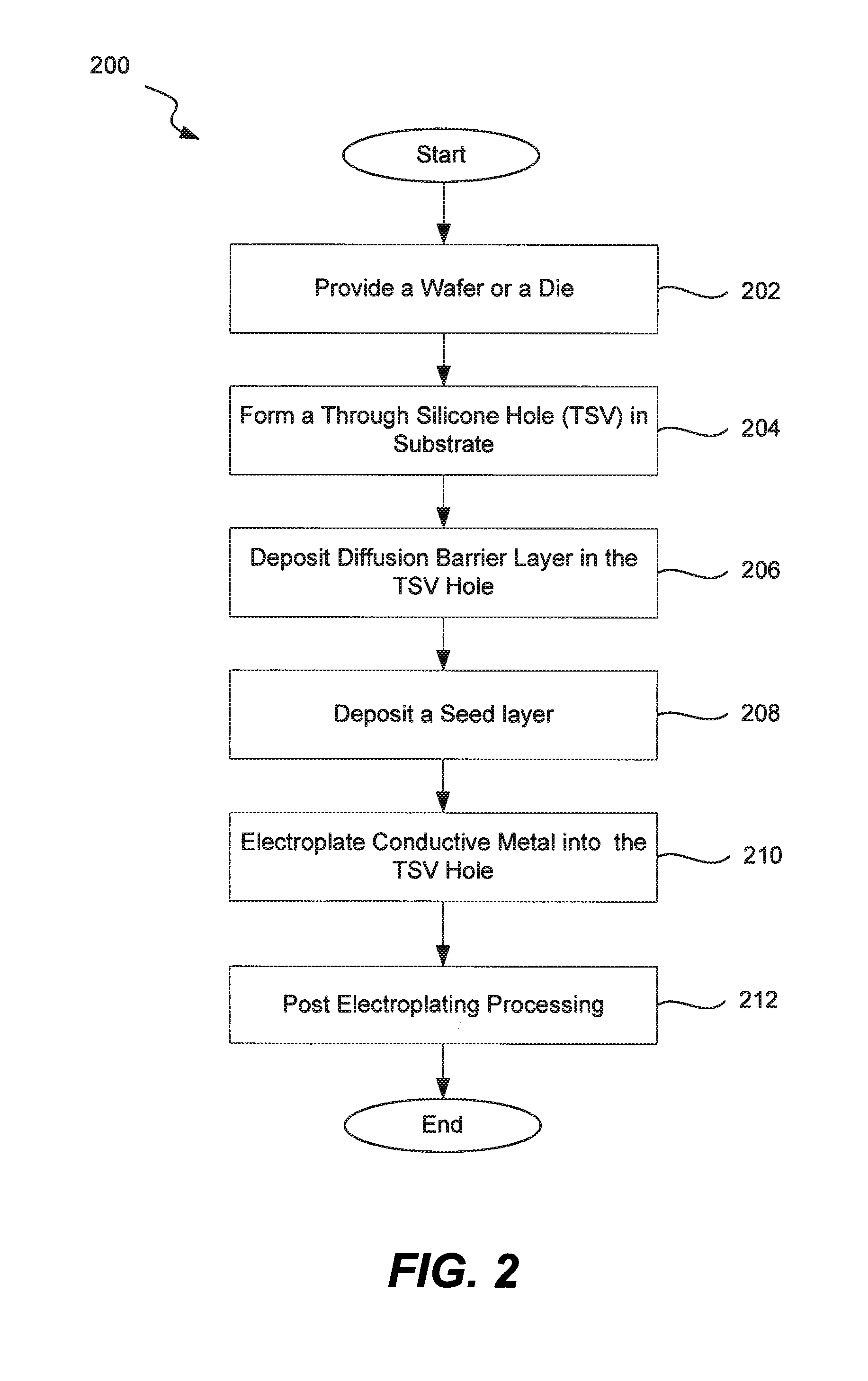
Process For Through Silicon Via Filling
a technology of silicon vias and filling processes, applied in electrolytic processes, solid-state devices, electrolysis components, etc., can solve the problems of difficult depositing of copper into such structures, limited step coverage, and high cost of precursors, and achieve high aspect ratio, fast copper migration, and large size
- Summary
- Abstract
- Description
- Claims
- Application Information
AI Technical Summary
Benefits of technology
Problems solved by technology
Method used
Image

Examples
examples
[0072]FIG. 7 presents the electroplating results for 25 micron deep 5 micron diameter TSV structures after plating for 1, 2, 3, and 4 minutes. Plating was performed at 60° C. using a solution at pH 3.5 containing 60 g / L concentration of copper ions, 3.5 ml / L Viaform accelerator (ATMI, Danbury, Conn.), 1 ml / L Viaform suppressor (ATMI, Danbury, Conn.), and 6 ml / L Extreme leveler (ATMI, Danbury, Conn.). No chloride ions were present in the solution. The wafer was placed into the bath without any current applied. The plating was performed in a bench-top plating cell using a typical agitation from a standard pump. FIG. 7 indicates that the copper first deposited on bottom of the TSV. Such distribution of copper deposition is highly beneficial and helps to prevent voids. FIG. 7 also indicates that no overburden was deposited in the regions between TSVs. Without being restricted to any particular theory, it is believed that localized corrosion cells may have been formed in between the TSV ...
PUM
| Property | Measurement | Unit |
|---|---|---|
| depth | aaaaa | aaaaa |
| diameter | aaaaa | aaaaa |
| concentration | aaaaa | aaaaa |
Abstract
Description
Claims
Application Information