Semiconductor storage device and methods of producing it

a technology of semiconductor storage and semiconductor layers, applied in semiconductor devices, electrical equipment, transistors, etc., can solve the problems of low thermal resistance of silicon layer, significant deterioration of transistor performance, and low transistor structure, and achieve the effect of reducing the occupied area

Active Publication Date: 2010-08-26
UNISANTIS ELECTRONICS SINGAPORE PTE LTD
View PDF8 Cites 99 Cited by
  • Summary
  • Abstract
  • Description
  • Claims
  • Application Information

AI Technical Summary

Benefits of technology

[0017]In view of the above circumstances, it is an object of the present invention to achieve a high-performance transistor in a peripheral circuit section of an SGT-DRAM having a memory cell area of 4F2 and a logic circuit section of a memory-embedded device, and achieve a transistor structure allowing for design of a circuit with a small occupied area.
[0031]As described above, in the semiconductor storage device and the memory-embedded semiconductor device of the present invention, a MOS transistor constituting the memory cell section and the peripheral circuit section and the logic circuit section is formed as a vertical transistor which comprises a planar semiconductor layer formed on a dielectric film on a substrate, a first impurity region formed in the planar semiconductor layer, a plurality of pillar-shaped semiconductor layers formed on the planar semiconductor layer, a second impurity region formed in an upper portion of each of the pillar-shaped semiconductor layers, and a gate formed on a side wall of each of the pillar-shaped semiconductor layers. Further, in the peripheral circuit section and the logic circuit section, a silicide layer is formed in a surface of the planar semiconductor layer to allow an N+ impurity region of an NMOS transistor and a P+ impurity region of a PMOS transistor to be directly connected to each other therethrough. This makes it possible to achieve a circuit having a reduced occupied area.

Problems solved by technology

Firstly, in view of high-performance requirements for a transistor in a peripheral circuit section of a DRAM and a logic circuit section of a DRAM-embedded device, it is contemplated to subject a source / drain diffusion layer to silicidation in order to reduce a parasitic resistance. However, in the above conventional example, a silicide layer must be formed in the source diffusion layer before forming a transistor. Generally, a silicide layer is low in thermal resistance. Thus, if a silicide layer is formed in the source diffusion layer and then a heat treatment required for forming a transistor is performed at about 1000° C., a resistivity of the silicide layer will become higher. Therefore, in the above conventional example, it is difficult to form in the source diffusion layer a silicide layer which contributes to a reduction in parasitic resistance.
Secondly, in the above conventional production method, the transistor-forming pillar-shaped silicon layer is made of polysilicon. This causes a significant deterioration in transistor performance, as compared with a conventional transistor where a channel region is made of single-crystal silicon.
As will be appreciated from the above description, the transistor structure of the peripheral circuit section disclosed in the Non-Patent Document 1 has significant difficultly in meeting the high-performance requirements for a transistor in a peripheral circuit section of a DRAM and a logic circuit section of a memory-embedded device.

Method used


Image

  • Semiconductor storage device and methods of producing it
  • Semiconductor storage device and methods of producing it
  • Semiconductor storage device and methods of producing it

Examples


first embodiment

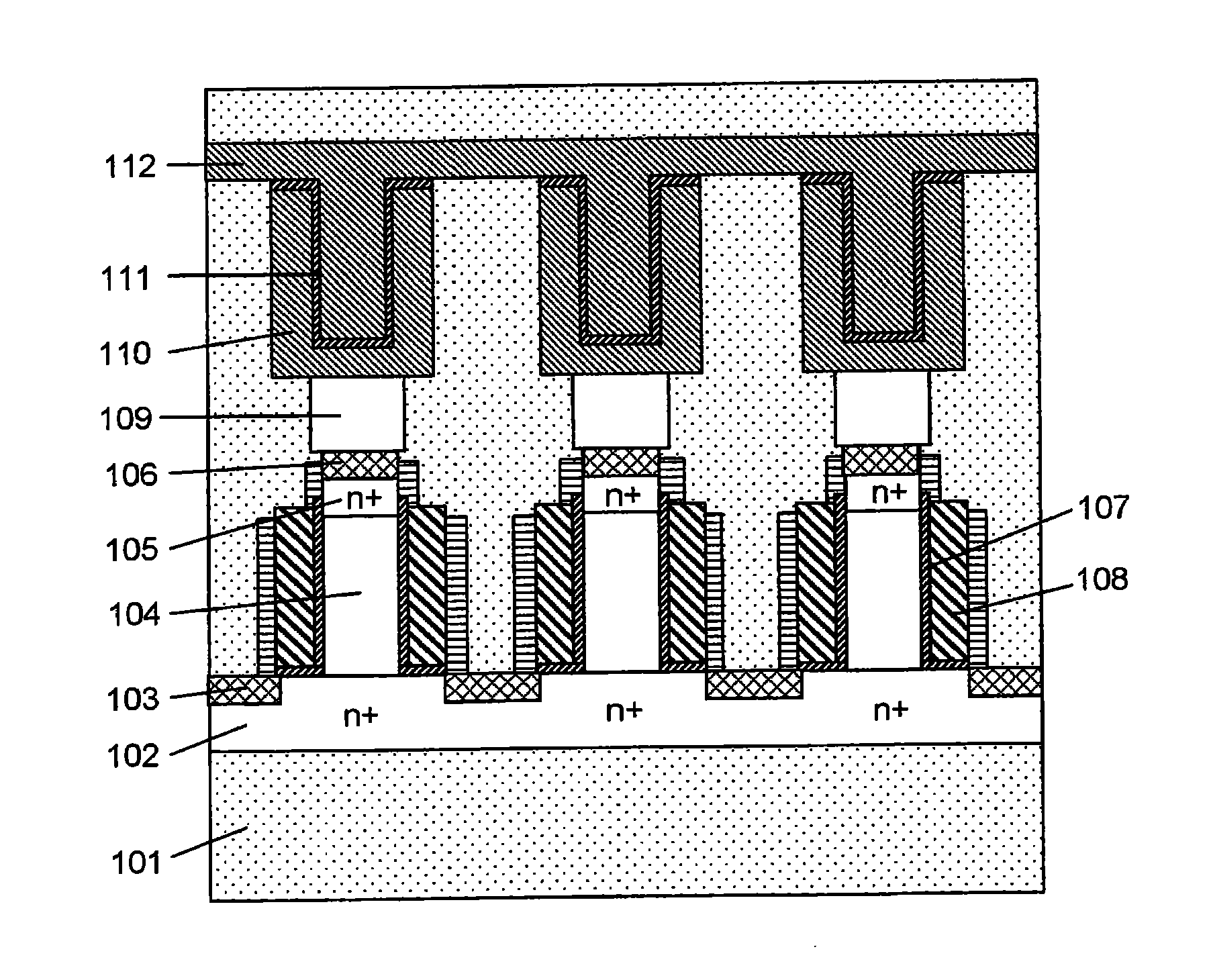
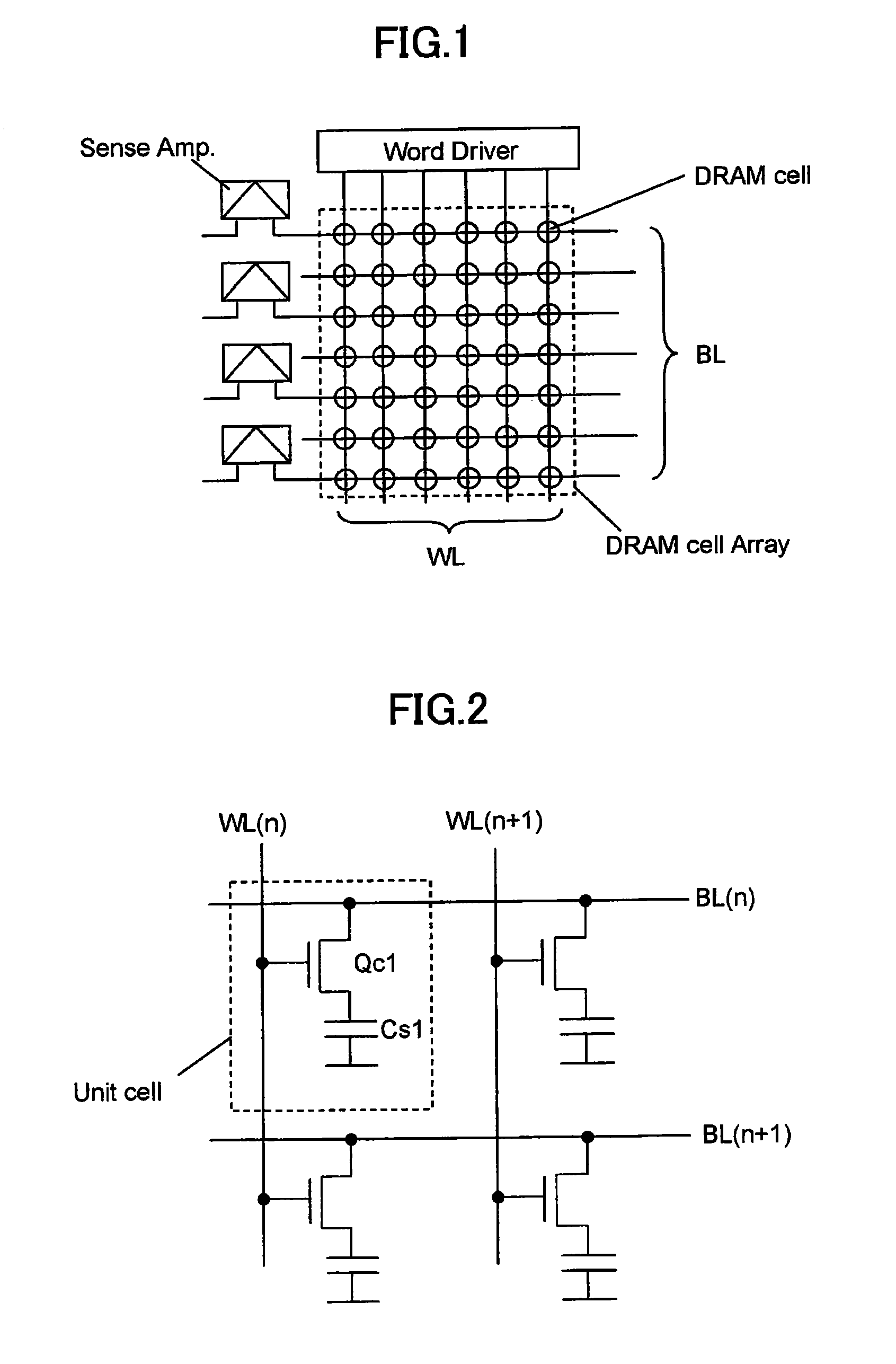
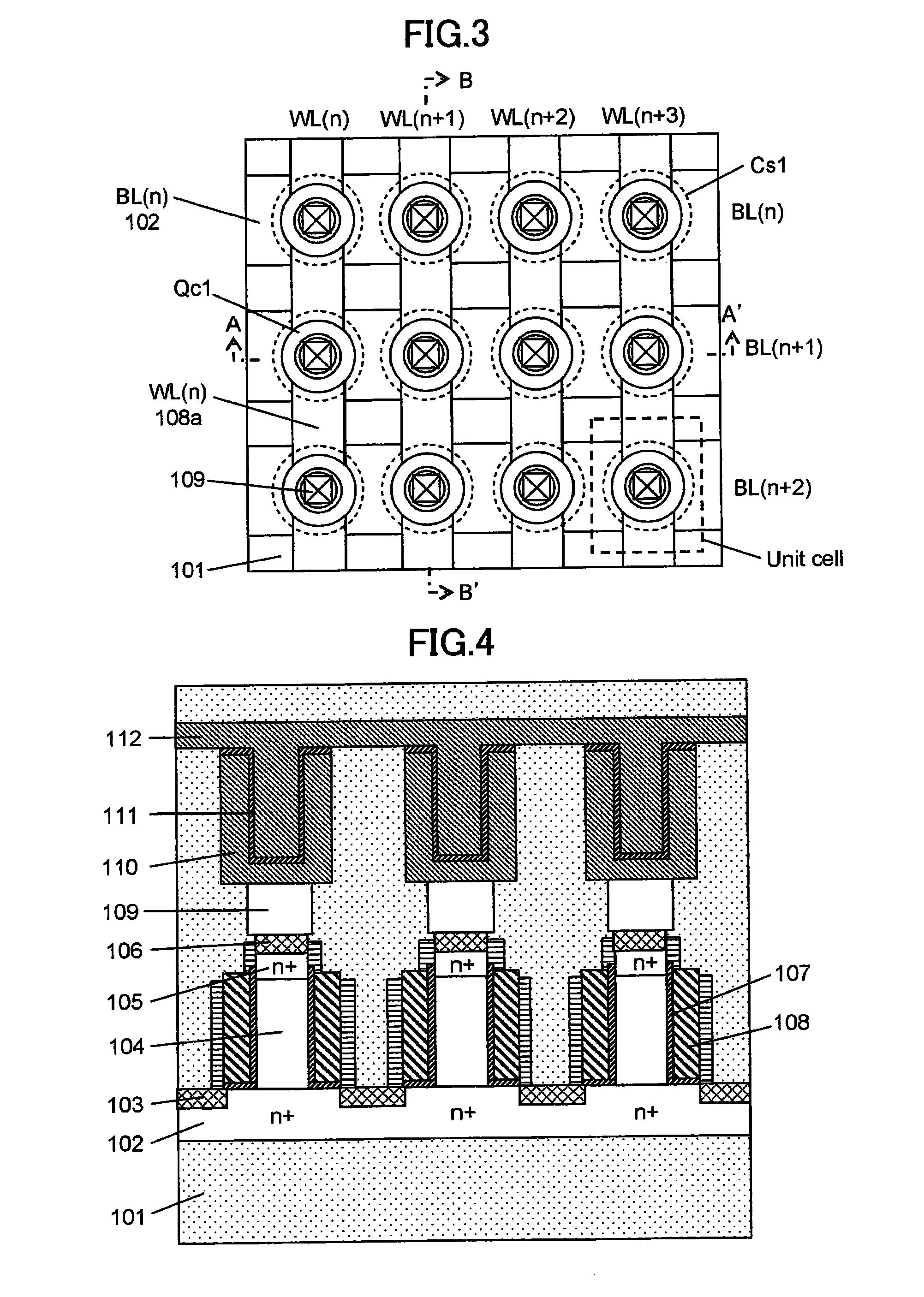
[0068]FIG. 1 illustrates a configuration of a cell array of a DRAM according to a first embodiment of the present invention. A plurality of DRAM cells are formed at respective ones of all a plurality of intersecting points of a plurality of bit lines with a plurality of word lines, to make up a cross-point type cell array. FIG. 2 illustrates an equivalent circuit of the DRAM cell formed at each of the intersecting points of the bit lines with the word lines. The DRAM cell comprises one capacitor element Cs1 operable to accumulate electric charges, and a selection transistor Qc1 operable to transfer electric charges. As a result of accumulating electric charges in the capacitor element Cs1, data is stored therein. Then, when a word line WL(n) associated with a gate electrode of the selection transistor Qc1 is turned on, the data stored in the capacitor element Cs1 is read out onto a bit line BL(n). The read-out signal is amplified by a sense amplifier connected to the bit line.

[0069]...

second embodiment

[0101]FIG. 24 is a sectional view showing a configuration of a CMOS inverter section according to a second embodiment of the present invention. Except a configuration of a CMOS circuit section, such as a CMOS inverter, in sectional view, the remaining configuration in the second embodiment is the same as that in the first embodiment.

[0102]In the first embodiment, the contact of the CMOS inverter section is formed in a two-layer structure. However, as a cell size of a DRAM becomes smaller, a height dimension of a capacitor element Cs1 has to be increased to adequately ensure an amount of electric charges to be accumulated, so that the second-layer contact 210 is increased in depth, which is likely to cause difficulty in forming the second-layer contact from a processed top surface. In this case, as shown in FIG. 24, the second-later contact 210 may be dividedly formed using a second-layer sub-contact 310a and a third-layer sub-contact 310b to facilitate formation of a contact. This c...

third embodiment

[0103]A third embodiment of the present invention provides a structure and a production method for a DRAM cell array section without silicidation. In the first embodiment, silicidation is also performed in the DRAM cell array section. However, the silicidation of the diffusion layer of the selection transistor in the DRAM cell is essentially required to increase an impurity concentration in the source / drain region, which causes deterioration in hold characteristics. The third embodiment can provide a DRAM having adequate hold characteristics, although the number of production processes is increased.

[0104]Except that no silicide layer is formed in a top surface of each of lower and upper diffusion layers, a configuration of the DRAM cell array section in top plan view is the same as that in FIG. 3.

[0105]With reference to FIGS. 25 and 26, the configuration of the DRAM cell array section will be described below. FIG. 25 is a sectional view taken along a cutting-plane line corresponding...


PUM


Abstract

The present invention provides a semiconductor storage device having a memory cell section and a peripheral circuit section each formed using one or more MOS transistors, comprising: a substrate; a dielectric film on the substrate; and a planar semiconductor layer formed on the on-substrate dielectric layer, wherein: the at least one MOS transistor in the memory cell section comprises a selection transistor, the at least one MOS transistor in the peripheral circuit section comprises a first MOS transistor and a second MOS transistor which are different in conductivity type from each other, the first MOS transistor includes a first lower drain or source region formed in the planar semiconductor layer, a first pillar-shaped semiconductor layer formed on the planar semiconductor layer, a first upper source or drain region formed in an upper portion of the first pillar-shaped semiconductor layer, and a first gate electrode formed such that the first gate electrode surrounds a sidewall of the first pillar-shaped semiconductor layer through a first dielectric film, the second MOS transistor includes a second lower drain or source region formed in the planar semiconductor layer, a second pillar-shaped semiconductor layer formed on the planar semiconductor layer, a second upper source or drain region formed in an upper portion of the second pillar-shaped semiconductor layer, and a second gate electrode formed such that the second gate electrode surrounds a sidewall of the second pillar-shaped semiconductor layer through a second dielectric film; and the selection transistor includes a third lower drain or source region formed in the planar semiconductor layer, a third pillar-shaped semiconductor layer formed on the planar semiconductor layer, a third lower source or drain region formed in an upper portion of the third pillar-shaped semiconductor layer, and a third gate electrode formed such that the third gate electrode surrounds a sidewall of the third pillar-shaped semiconductor layer through a third dielectric film, and wherein the semiconductor storage device has a first silicide layer formed thereon to connect at least a part of a surface of the first lower drain or source region of the first MOS transistor and at least a part of a surface of the second lower drain or source region of the second MOS transistor, and a second silicide layer formed on at least a part of a surface of the third lower drain or source region of the selection transistor.

Description

RELATED APPLICATIONS[0001]Pursuant to 35 U.S.C. §119(e), this application claims the benefit of the filing date of Provisional U.S. Patent Application Ser. No. 61 / 207,652 filed on Feb. 13, 2009. This application is a continuation application of PCT / JP2009 / 051463 filed on Jan. 29, 2009 which claims priority under 35 U.S.C. §365(a) to PCT / JP2008 / 051304 filed on Jan. 29, 2008. The entire contents of these applications are hereby incorporated by reference.TECHNICAL FIELD[0002]The present invention relates to a semiconductor device and a production method therefor, and more particularly to a semiconductor storage device such as a DRAM, a memory-embedded semiconductor device having embedded therein a logic circuit section and a memory section such as a DRAM, and methods of producing it.BACKGROUND ART[0003]With a view to achieving higher integration and higher performance of an LSI device, an SGT (Surrounding Gate Transistor) has been proposed which comprises a pillar-shaped semiconductor ...

Claims


Application Information

Patent Timeline
Patent Type & Authority Applications(United States)
IPC IPC(8): H01L27/108H01L21/8242H01L27/088
CPCH01L21/823828H01L27/10894H01L27/10876H01L21/823885H10B12/053H10B12/09
Inventor MASUOKA, FUJIOARAI
Owner UNISANTIS ELECTRONICS SINGAPORE PTE LTD
Why Eureka
Try Eureka