

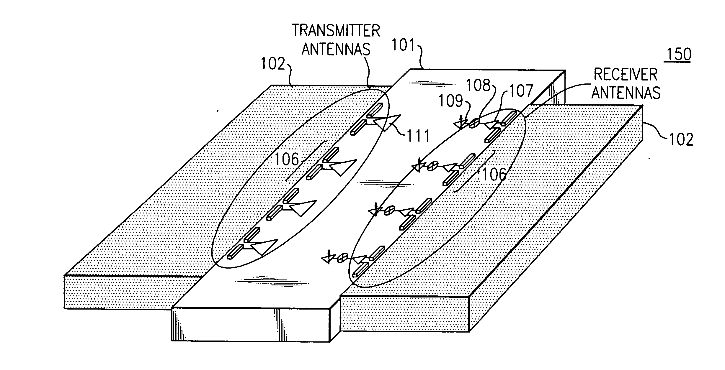
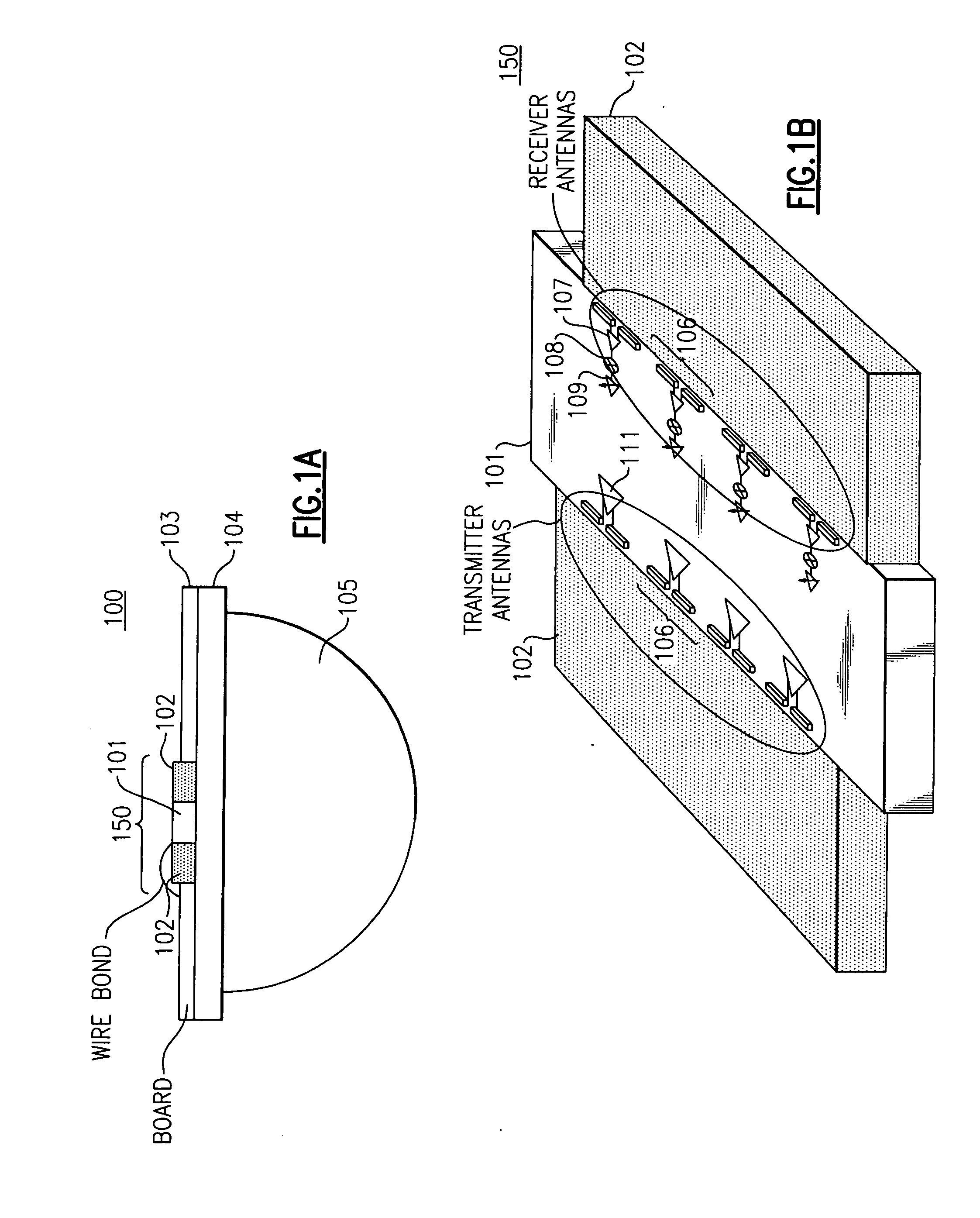
Mm-wave fully integrated phased array receiver and transmitter with on-chip antennas
a phased array, fully integrated technology, applied in the direction of antennas, instruments, antenna feed intermediates, etc., can solve the problems of substrate dielectric loss, difficulty in detecting and the difficulty of coupling power output from an integrated mm-wave transmitter to an off-chip radiating device, etc., to achieve the effect of improving the transmission or reception of mm-waves
- Summary
- Abstract
- Description
- Claims
- Application Information
AI Technical Summary
Benefits of technology
Problems solved by technology
Method used
Image

Examples
example 1
[0094]Several sections of an exemplary mm-wave fully integrated phased array receiver with on-chip antenna are now explained in more detail.
I. Antenna Simulations and Measurement
[0095]IE3D (a MoM-based electromagnetic simulator, available from Zeland Software, Inc., 48834 Kato Road, 103A, Fremont, Calif. 94538; see http: / / www.zeland.com) and HFSS (3D electromagnetic-field simulation software for high-performance electronic design, available from Ansoft Corporation, 225 West Station Square Drive, Suite 200, Pittsburgh, Pa. 15219; see http: / / www.ansoft.com / products / hf / hfss / ) were used to simulate antenna pattern and impedance. The effects of reflection from chip edge, coupling between antenna and its feeding T-lines, metal filling and coupling between adjacent antennas were all simulated. IE3D was used to model the T-lines. FIG. 10 shows an IE3D prototype used to simulate one of the T-line structures of an LNA. The IE3D extracted S-parameters of T-lines can be used in ADS for circuit ...
example 2
[0112]Transmitter chip performance was measured using a combination of waveguide-based probing and self-test mechanisms incorporated in the chip. At all high-frequency measurement points, the pads were incorporated into a tapered coplanar waveguide structure, thereby accounting for pad parasitics while maintaining a 50Ω impedance. For instance, both VCO and divide-by-two outputs were connected to such pad structures to enable direct measurement. The VCO can be tuned from 50.35 GHz to 55.49 GHz, while the locking range of the divider is 51.4 GHz to 54.5 GHz which is sufficient for our application.
[0113]As shown in FIG. 21, a transmitter was characterized using a waveguide probe that was followed by an external downconverter (with a 59 GHz LO). The transmitter generates up to +10.1 dBm output power at 77 GHz and has 34 dB of gain from baseband to RF with a bandwidth of 2.2 GHz.
Loopback Testing
[0114]In order to test the raw beam-performing abilities of the transmitter, excluding the on...
example 3
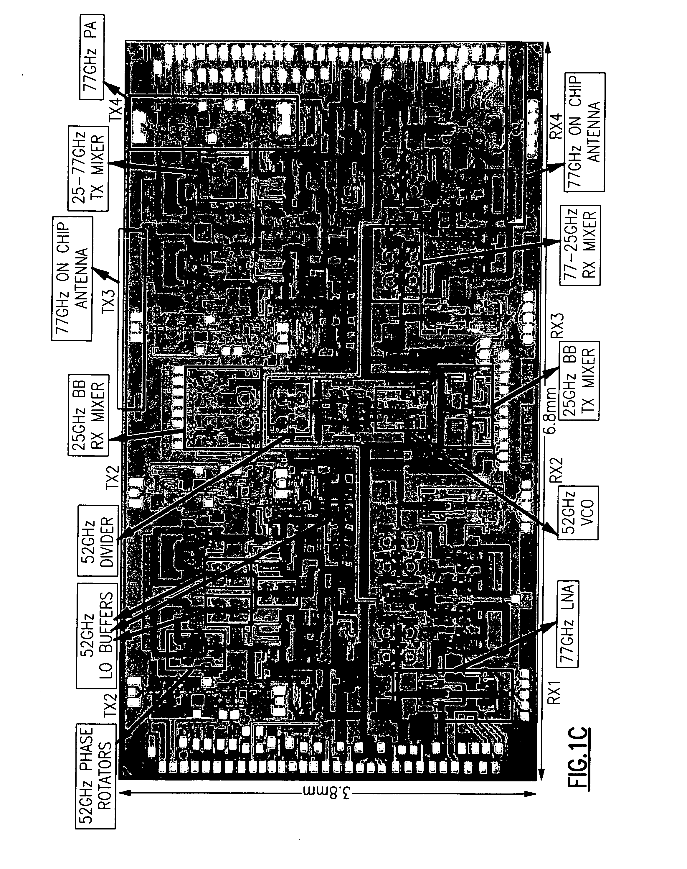
[0115]FIG. 22A through FIG. 22D show the measured patterns with 2 transmit-receive pairs active in the loopback mode which demonstrates the beam-forming capabilities of the transmitter. The transmitter was implemented in a 0.12 μm SiGe BiCMOS process with seven metal layers. The performance of the phased-array transmitter is summarized in table shown in FIG. 23. The transmitter and local phase shifting occupy 17 mm2 of die area (FIG. 24).
PUM
 Abstract
Description
Claims
Application Information