Compound semiconductor substrate

Inactive Publication Date: 2010-09-30
COORSTEK INC
View PDF13 Cites 13 Cited by
  • Summary
  • Abstract
  • Description
  • Claims
  • Application Information

AI Technical Summary

Benefits of technology

[0018]According to the invention, there is provided a compound semiconductor substrate which is capable of inhibiting ni

Problems solved by technology

Furthermore, since the difference in crystal lattice constant between silicon and the nitride semiconductors is as large as 10% or more, there is a problem that the difference causes crystal defects, etc.
However, there is a problem that formation of a thick buffer layer and a thick nitride semiconductor layer on a single-crystal silicon substrate by epitaxial

Method used


Image

  • Compound semiconductor substrate
  • Compound semiconductor substrate
  • Compound semiconductor substrate

Examples


Example

Example 1

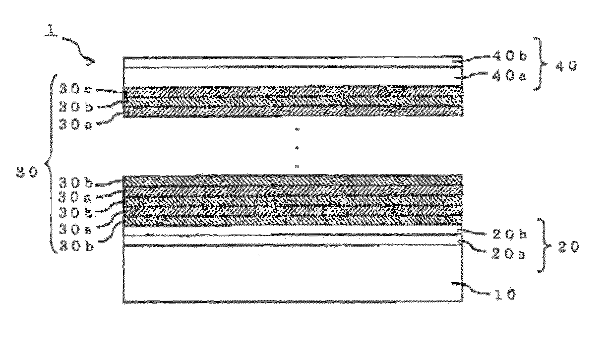
[0059]A single-crystal silicon substrate 10 having a diameter of 4 inches and a thickness of 500 μm, which had a crystal face with (111) orientation and a carrier density of 1×10¹⁸ / cm3 and showed n-type conduction and which had been produced by the CZ method and mirror-polished on one side, was heat-treated at 1,000° C. in a hydrogen atmosphere to clean the surface.

[0060]Subsequently, the substrate temperature was adjusted to 1,150° C., and TMA (trimethylaluminum) and NH3 (ammonia) gas were fed to form an AlN unit layer having a thickness of 100 nm and constituted of an MN single crystal (20a in FIG. 1) on the polished surface of the single-crystal silicon substrate 10. Next, the substrate temperature was adjusted to 1,050° C., and TMG (trimethylgallium) was further fed. The feed amounts of TMA and TMG were regulated to form an AlGaN unit layer having a thickness of 200 nm and constituted of an Al0.2Ga0.8N single crystal (20b in FIG. 1) on the AlN unit layer.

[0061]Subsequen...

Example

Comparative Example 1

[0066]A plurality of samples were produced in the same manner as in Example 1, except that the thickness of each second unit layer 30b was regulated to 1 nm.

[0067]The compound semiconductor substrates thus produced were examined for the occurrence of cracks in the same manner as in Example 1. As a result, visually recognizable cracks were observed in the surface of the AlGaN layer 40b of each sample.

Example

Comparative Example 2

[0068]A plurality of samples were produced in the same manner as in Example 1, except that the thickness of each second unit layer 30b was regulated to 30 nm.

[0069]The compound semiconductor substrates thus produced were examined for the occurrence of cracks in the same manner as in Example 1. As a result, small cracks were observed in the surface of the AlGaN layer 40b of each sample. Warpage was also measured in the same manner as in Example 1. As a result, the warpage was found to be about 40 μm. It was ascertained that the warpage itself was approximately the same as in Example 1.


PUM

PropertyMeasurementUnit
Nanoscale particle sizeaaaaaaaaaa

Abstract

The present invention provides a compound semiconductor substrate, including: a single-crystal silicon substrate having a crystal face with (111) orientation; a first buffer layer which is formed on the single-crystal silicon substrate and is constituted of an AlxGa1-xN single crystal (0<x≦1); a second buffer layer which is formed on the first buffer layer and is composed of a plurality of first unit layers each having a thickness of from 250 nm to 350 nm and constituted of an AlyGa1-yN single crystal (0≦y<0.1) and a plurality of second unit layers each having a thickness of from 5 nm to 20 nm and constituted of an AlzGa1-zN single crystal (0.9<z≦1), said pluralities of first and second unit layers having been alternately superposed; and a semiconductor device formation region which is formed on the second buffer layer and includes at least one nitride-based semiconductor single-crystal layer. The compound semiconductor substrate according to the invention is suitable for use in electronic devices such as HEMTs (high electron mobility transistors).

Description

FIELD OF THE INVENTION[0001]The present invention relates to a compound semiconductor substrate suitable for use in electronic devices such as HEMTs (high electron mobility transistors) and the like.BACKGROUND OF THE INVENTION[0002]Nitride semiconductors represented by gallium nitride (GaN), aluminum nitride (AlN), and the like have a higher electron mobility and a wider band gap than silicon, and are expected to be used for implementing an electronic device taking advantage of those features, such as a very-high-speed transistor or a very-low-loss switching device. Because of such excellent material properties, devices employing nitride semiconductors are expected to surpass the devices based on semiconductor silicon, which are mainly used at present, in material-property limit.[0003]As substrates for the epitaxial growth of such a nitride semiconductor thereon, use has hitherto been made of sapphire, silicon (Si), silicon carbide (SiC), zinc oxide (ZnO), and the like. Of these sub...

Claims


Application Information

Patent Timeline
IPC IPC(8): H01L29/20
CPCC23C16/303C30B25/183C30B29/403H01L21/02381H01L21/02433C23C16/0272H01L21/02507H01L21/0254H01L29/2003H01L29/7787H01L21/02458
Inventor OISHI, HIROSHIKOMIYAMA, JUNERIGUCHI, KENICHIABE, YOSHIHISAYOSHIDA, AKIRASUZUKI, SHUNICHI
Owner COORSTEK INC
Why Eureka
Try Eureka