Sulfurization or selenization in molten (liquid) state for the photovoltaic applications

a photovoltaic and liquid state technology, applied in the field of compound semiconductor material formation, can solve the problems of hazardous sulfurization and selenization processes, affecting the quality of photovoltaic cells,

Inactive Publication Date: 2010-10-07
APPLIED MATERIALS INC
View PDF11 Cites 18 Cited by
  • Summary
  • Abstract
  • Description
  • Claims
  • Application Information

AI Technical Summary

Benefits of technology

[0011]Further embodiments provide a method of forming a compound semiconductor, comprising depositing a molybdenum layer on a substrate by physical vapor deposition, depositing a copper-indium-gallium alloy layer on the molybdenum layer by physical vapor deposition, heating the substrate to a temperature of at least 400° C., contacting the copper-indium-gallium alloy layer with liquid bath comprising one or more group VI elements, diffusing an excess amount of the one or more group VI elements into the copper-indium-gallium alloy layer and reacting the one or more group VI elements with the copper-indium-gallium alloy layer, and reducing the excess of group VI elements by volatilizing the excess group VI elements in an annealing process.

Problems solved by technology

Compounds used today in sulfurization and selenization processes are hazardous.
Hydrogen selenide is quite toxic, and both hydrogen selenide and hydrogen sulfide can degrade process equipment, and may be incompatible with some substrate materials.
Additionally, vapor exposure processes have high material utilization rates, because most of the vapor is not incorporated into the substrate.
Also, solar cells formed using vapor techniques frequently have reduced performance characteristics due to high defect densities and incorporation of hydrogen.
Processes developed to address the performance issues, such as thermal co-evaporation, are inefficient due to low throughput and high material utilization.

Method used


Image

  • Sulfurization or selenization in molten (liquid) state for the photovoltaic applications
  • Sulfurization or selenization in molten (liquid) state for the photovoltaic applications
  • Sulfurization or selenization in molten (liquid) state for the photovoltaic applications

Examples


Embodiment Construction

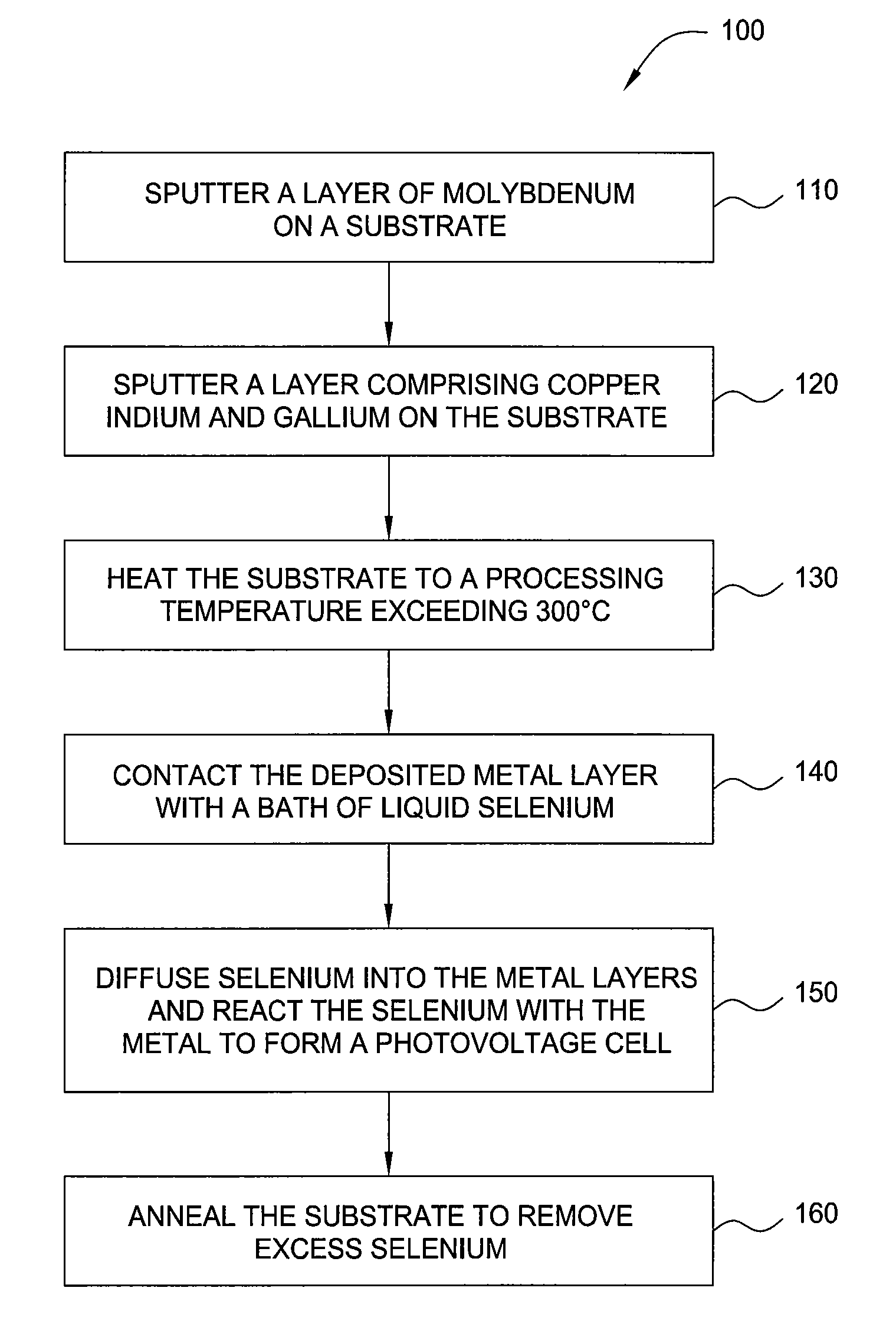
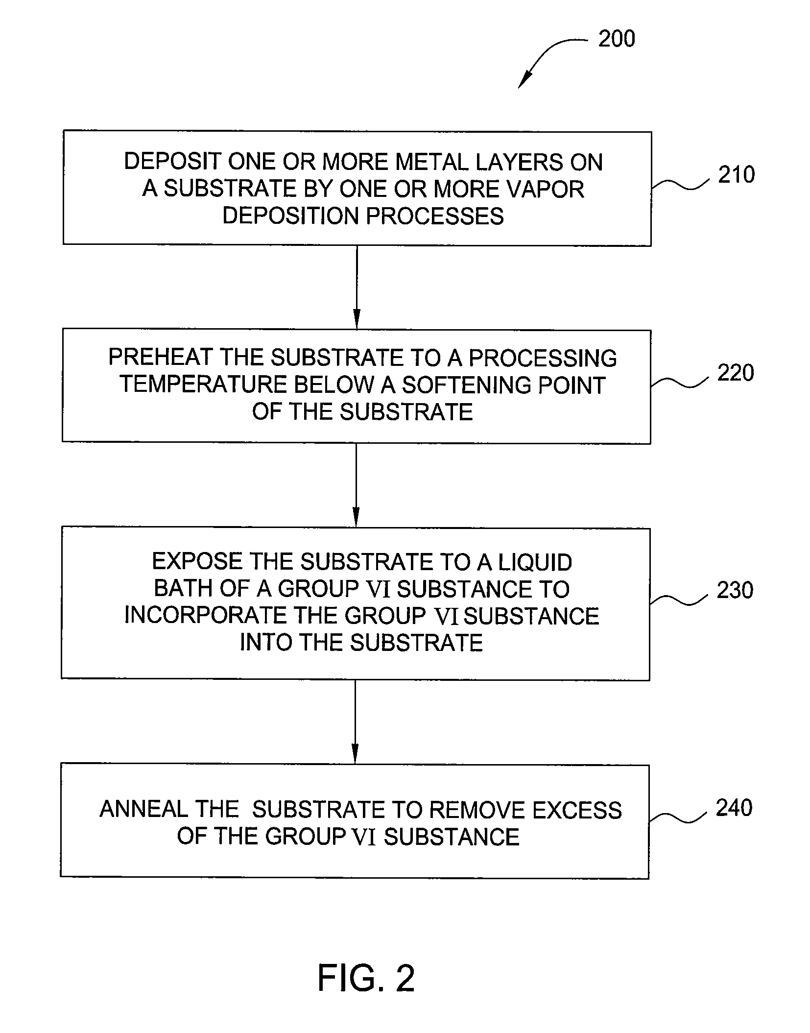
[0017]Embodiments of the invention generally provide a method of incorporating a chemical component into a solar cell substrate. Methods described herein are generally useful for fabricating so-called II / VI compound semiconductors, which have uses in solar panel and integrated circuit applications. Compounds in this group generally comprise components selected from the group consisting of copper, indium, gallium, molybdenum, thallium, zinc, mercury, boron, aluminum, silver, sulfur, selenium, and tellurium. In solar and I / C applications, these compounds are generally formed on a substrate as thin films having near-stoichiometric quantities of the “group II” components (Cu, In, Ga, TI, Zn, Hg, B, Al, Ag) with one or more of the “group VI” components (S, Se, Te). While metals in the zinc column of the periodic table are frequently used alone as the group II component (e.g. CdS, CdSe), elements on one side of the zinc column are frequently combined with elements on the other side to pro...


PUM

PropertyMeasurementUnit
temperatureaaaaaaaaaa
thickaaaaaaaaaa
thickaaaaaaaaaa

Abstract

A method of forming a solar cell incorporating a compound semiconductor is provided. The compound semiconductor is generally of the “II/VI” variety, and is formed by depositing one or more group II elements in a vapor deposition process, and then contacting the deposited layer with a liquid bath of the group VI elements. The liquid bath may comprise a pure element or a mixture of elements. The contacting is performed under a non-reactive atmosphere, or vacuum, and any fugitive vapors may be captured by a cold trap and recycled. The substrate may be subsequently annealed to remove any excess of the group VI elements, which may be similarly recycled.

Description

CROSS-REFERENCE TO RELATED APPLICATIONS[0001]This application claims benefit of U.S. Provisional Patent Application Ser. No. 61 / 167,449 filed Apr. 7, 2009, which is herein incorporated by reference.BACKGROUND OF THE INVENTION[0002]1. Field of the Invention[0003]Embodiments of the invention relate to formation of compound semiconductor materials. More specifically, embodiments of the invention relate to methods of forming compound semiconductors having a group VI element.[0004]2. Description of the Related Art[0005]Increasing focus on renewable sources of energy have led to development of many types of solar cells involving semiconductors as energy absorbers. Although silicon-based solar cells are the most common, one increasingly common type of semiconductor used in thin film solar cells is the compound semiconductor. Compound materials formed from so-called “II / VI” mixtures generally have semiconducting properties useful for solar cell energy absorber layers. Examples of such mater...

Claims


Application Information

Patent Timeline
Patent Type & Authority Applications(United States)
IPC IPC(8): H01L21/363
CPCC23C14/025C23C14/165C23C14/185C23C14/5866Y02E10/541H01L21/02565H01L21/02568H01L21/02614H01L31/0322H01L21/02551
Inventor SINGH, KAUSHAL K.HOFMANN, RALFKRISHNA, NETY M.
Owner APPLIED MATERIALS INC
Why Eureka
Try Eureka