Massively Parallel Interconnect Fabric for Complex Semiconductor Devices

a technology of interconnect fabric and semiconductor device, which is applied in the direction of semiconductor device, semiconductor/solid-state device details, electrical apparatus, etc., can solve the problems of less area and power consumption of core die substrate parts, and achieve the effect of reducing production cost, reducing associated resources and skill sets, and reducing the cost of ic developmen

Active Publication Date: 2010-11-11
BEMANIAN MAJID +1
View PDF10 Cites 75 Cited by
  • Summary
  • Abstract
  • Description
  • Claims
  • Application Information

AI Technical Summary

Benefits of technology

[0009]In an embodiment of this invention, system on chip (SOC) macro blocks are separated and used as building blocks for SOC construction via MPIF, with e.g., processors (general and custom), memory, analog functions, specialty I/O, digital signal processing (DSP). The decoupling of core and context of SOC architecture and implementation, in an embodiment of this invention, reduces the cost of IC development drastically, due to reduction of integration of the building blocks (context), reduction in associated resources and skill set for coding (R&D), verification, and test. In one embodiment, the production cost is reduced, for example, due to increase in overall yield. In one embodiment, the area, power consumption is reduced due to core stacking at the gate l

Problems solved by technology

For example, in the case of FPGA, since the interconnects and storage elements are separated from the core LE (

Method used


Image

  • Massively Parallel Interconnect Fabric for Complex Semiconductor Devices
  • Massively Parallel Interconnect Fabric for Complex Semiconductor Devices
  • Massively Parallel Interconnect Fabric for Complex Semiconductor Devices

Examples


Embodiment Construction

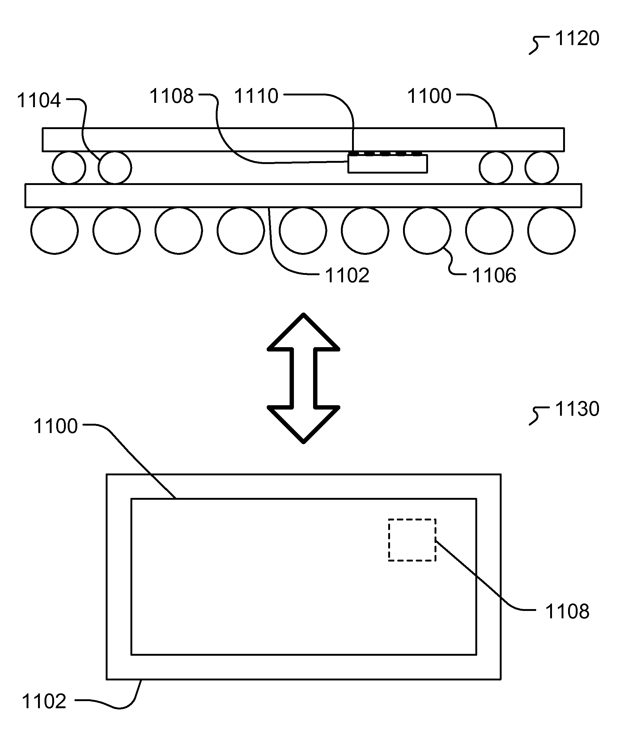
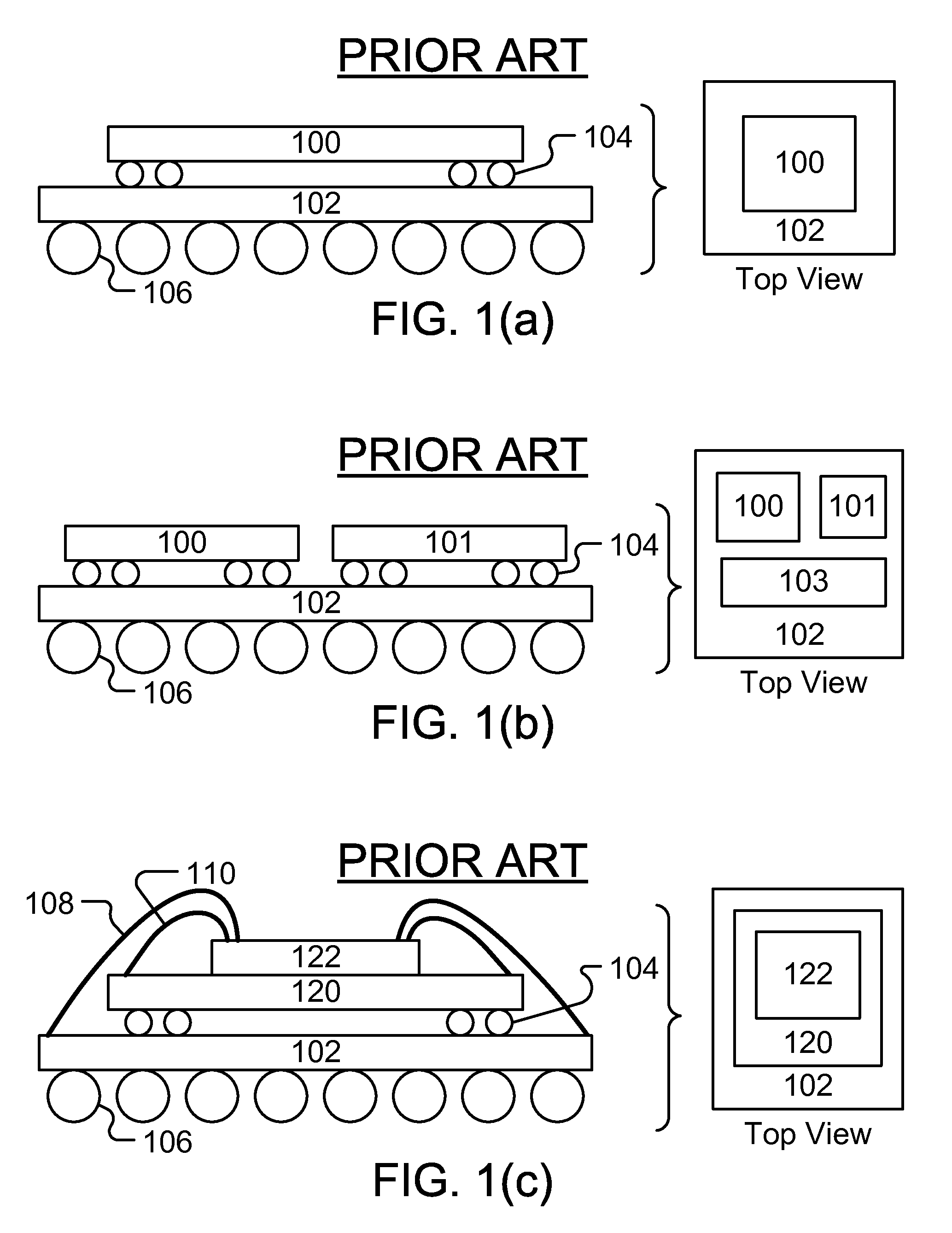
[0041]Flip-chip or wire bonding techniques are commonly used in semiconductor packaging of semiconductor devices (on die) to package substrate. However, these techniques are typically used at SOC / chip / I / O level (i.e., higher hierarchical interconnect level) given the size and other physical and design requirements / constraints, instead of gate / logic block level (i.e., lower hierarchical interconnect level). In such an interconnect hierarchy, the inter-gate level connections tend to be localized at micro level; inter-micro level connections tend to be localized at macro level; and the inter-macro level connections tend to be localized at chip / SOC level. Therefore, even though there may be millions of gate level connections, e.g., in a SOC, there are much fewer chip-chip interconnects.

[0042]For example, FIG. 1(a) illustrates a prior art the flip-chip placement of a die (100) on a package substrate (102) using die bumps (104) placed on the die for electrical connection between the die ...


PUM


Abstract

An embodiment of this invention uses a massive parallel interconnect fabric (MPIF) at the flipped interface of a core die substrate (having the core logic blocks) and a context die (used for in circuit programming/context/customization of the core die substrate), to produce ASIC-like density and FPGA-like flexibility/programmability, while reducing the time and cost for development and going from prototyping to production, reducing cost per die, reducing or eliminating NRE, and increasing performance. Other embodiments of this invention enable debugging complex SoC through large contact points provided through the MPIF, provide for multi-platform functionality, and enable incorporating FGPA core in ASIC platform through the MPIF.

Description

BACKGROUND OF THE INVENTION[0001]Two prevalent approaches for building complex custom semiconductor devices are based on field-programmable gate array (FPGA) or application-specific integrated circuit (ASIC).[0002]A FPGA is a semiconductor device that can be configured by the customer or designer after manufacturing, using a logic circuit diagram or a source code in a hardware description language (HDL) describing how the chip functions. FPGAs contain programmable logic components (logic blocks), and a hierarchy of reconfigurable interconnects that allow the blocks to be wired together. Logic blocks can be configured to perform complex combinational functions as well as simple logic gates through combinational logic and / or lookup table(s). In FPGAs, the logic blocks may include memory elements in form of simple flip-flops or even more complete blocks of memory.[0003]An ASIC is an integrated circuit (IC) customized for a particular use, rather than intended for general-purpose use. T...

Claims


Application Information

Patent Timeline
IPC IPC(8): H01L29/66
CPCH01L23/13H01L2224/16225H01L24/14H01L24/16H01L24/48H01L25/0652H01L25/0655H01L25/0657H01L25/18H01L2223/6677H01L2224/13099H01L2224/16227H01L2224/48145H01L2224/48227H01L2225/06513H01L2225/06517H01L2225/0652H01L2225/06527H01L2225/06541H01L2225/06572H01L2225/06589H01L2924/01029H01L2924/01058H01L2924/01079H01L2924/01082H01L2924/10329H01L2924/15321H01L2924/15331H01L2924/01005H01L2924/01006H01L2924/01019H01L2924/01033H01L2924/01075H01L2924/01087H01L2924/014H01L2924/3511H01L2924/30107H01L23/525H01L2924/00H01L2924/181H01L2924/14H01L2924/00014H01L2224/45099H01L2224/45015H01L2924/207H01L2924/00012
Inventor BEMANIAN, MAJIDYAZDANI, FARHANG
Owner BEMANIAN MAJID
Why Eureka
Try Eureka