

Method of preparing bundle type silicon nanorod composite through electroless etching process using metal ions and anode active material for lithium secondary cells comprising the same
a technology of metal ions and anodes, which is applied in the direction of non-metal conductors, cell components, conductors, etc., can solve the problems of reducing the capacity of silicon anodes, reducing the inner stress of silicon occurring reducing the inner stress of silicon at the time of charging and discharging a cell, so as to prevent the deterioration of an electrode, stably maintain a cell capacity
- Summary
- Abstract
- Description
- Claims
- Application Information
AI Technical Summary
Benefits of technology
Problems solved by technology
Method used
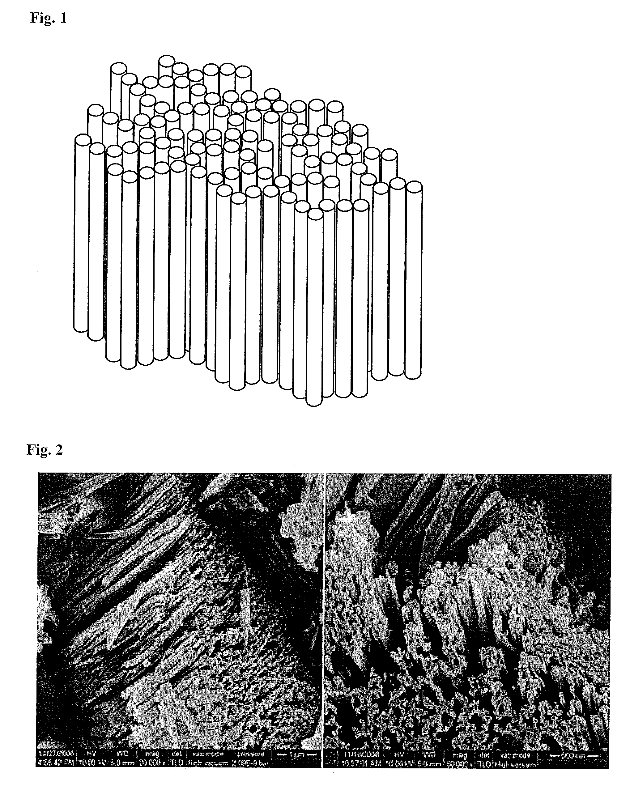
Image

Examples
example 1
Preparation of a Silcon Anode Active Material Electrodeposited with Silver
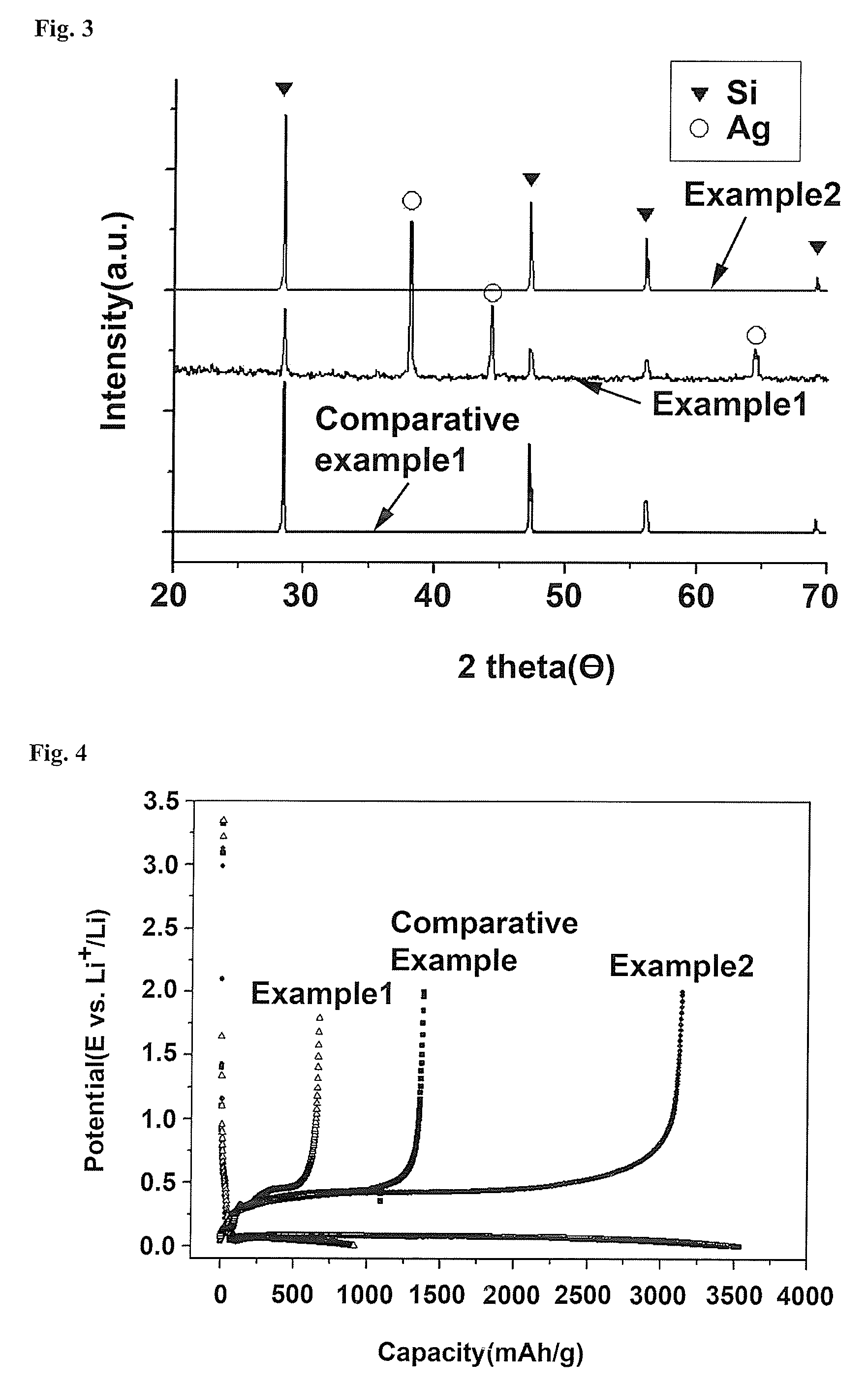
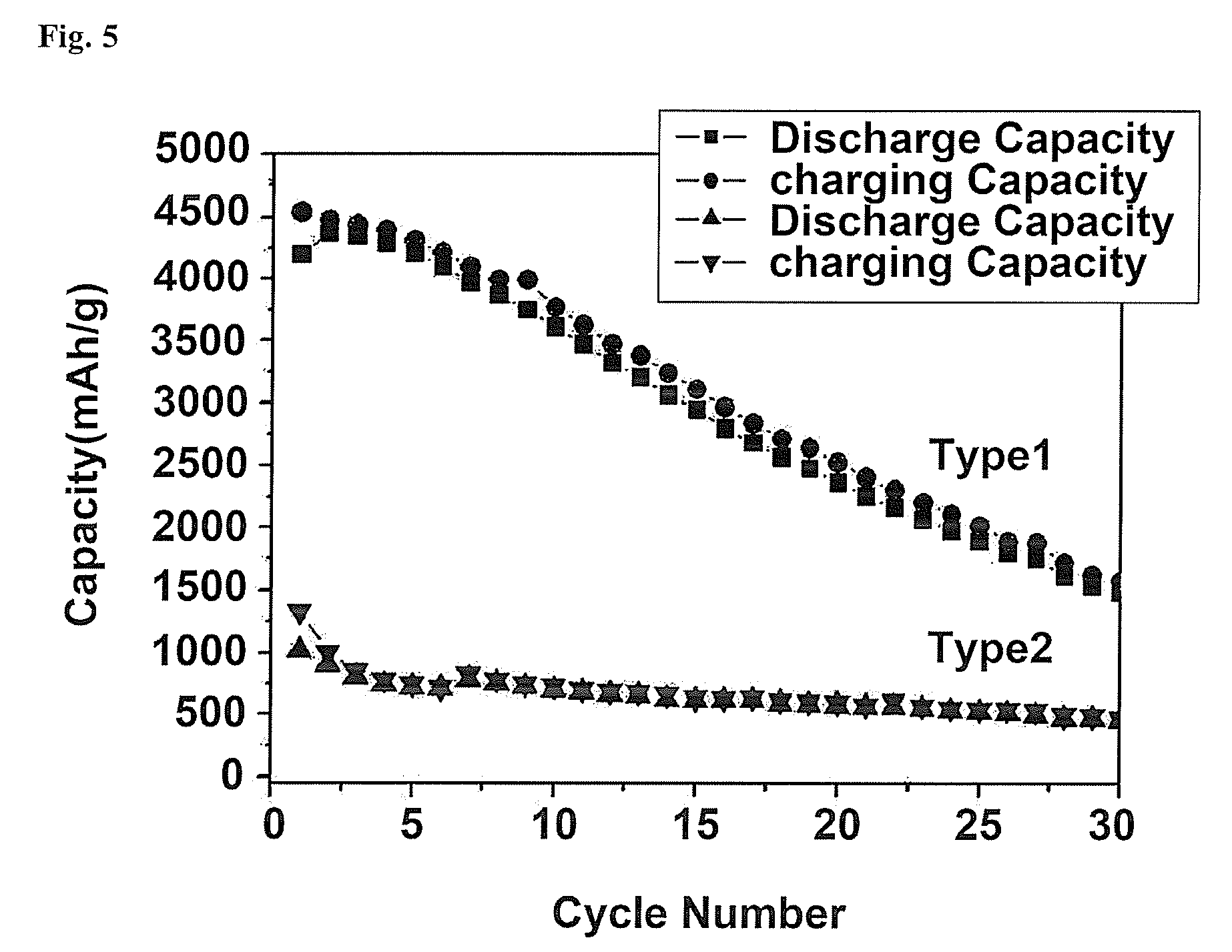
[0044]6.14 g of AgNO3 and 87 mL of HF (48-52%) were mixed in 813 mL of distilled water, and then stirred for about 10 minutes to form a mixed solution. Subsequently, 100 mL of distilled water and 2 g of silicon powder (ca. 2.5 μm, manufactured by Kojundo Corp.) were put into a reactor and then ultrasonically dispersed, and then the mixed solution was put into the reactor and then stirred for 1 hour to obtain particles. The obtained particles were passed through a filter to remove the reaction solution, and then washed with 1000 mL of distilled water to remove unreacted impurities therefrom using filter paper.
example 2
Preparation of a Silicon Anode Active Material from Which wlectrodeposited Silver is Removed
[0045]6.14 g of AgNO3 and 87 mL of HF (48-52%) were mixed in 813 mL of distilled water, and then stirred for about 10 minutes to form a mixed solution. Subsequently, 100 mL of distilled water and 2 g of silicon powder (ca. 2.5 μm, manufactured by Kojundo Corp.) were put into a reactor and then ultrasonically dispersed, and then the mixed solution was put into the reactor and then stirred for 1 hour at 5° C. -100° C. to proceed reduction / oxidation reactions from (1) to (3) on the surface of the silicon particles. Under the experimental range, the pore diameter decreases with the increase of reaction temperature and vice versa. The reaction temperature, therefore, affect affects the surface morphology of the silicon. The obtained particles were passed through a filter to remove the reaction solution, and then washed with 1000 mL of distilled water to remove unreacted impurities therefrom using ...
example 3
Manufacture of an Anode
[0047]Anodes were manufactured using the silicon anode active materials prepared in Examples 1 and 2 and the silicon powder of Comparative Example 1, respectively.
[0048]As an organic binder of the silicon anode active materials prepared in Examples 1 and 2 and the silicon powder of Comparative Example 1, a polymer solution including N-methyl-pyridone (NMP) and 5% of poly vinylidene fluoride (PVdF) was used. 15% by weight of carbon black, serving as a conductive material, was added to an electrode including 70% by weight of the silicon anode active material and 15% by weight of the organic binder in order to decrease the resistance of the electrode. In this case, a pure organic NMP solvent was added to the mixture including the silicon anode active material, organic binder and conductive material such that its weight is a half of the weight of the mixture, and then stirred at a high rotation speed of 5000 rpm for 30 minutes to obtain a slurry having appropriate...
PUM
| Property | Measurement | Unit |
|---|---|---|
| Temperature | aaaaa | aaaaa |
| Length | aaaaa | aaaaa |
| Length | aaaaa | aaaaa |
Abstract
Description
Claims
Application Information