

Monitoring of electroplating additives
a technology of additives and electroplating, applied in the direction of liquid/fluent solid measurement, material electrochemical variables, instruments, etc., can solve the problems of large footprint, large size and large footprint of detection and analysis equipment, and the inability to change the solution studied while a measurement is being completed, etc., to achieve the effect of small footprin
- Summary
- Abstract
- Description
- Claims
- Application Information
AI Technical Summary
Benefits of technology
Problems solved by technology
Method used
Image

Examples
example 1
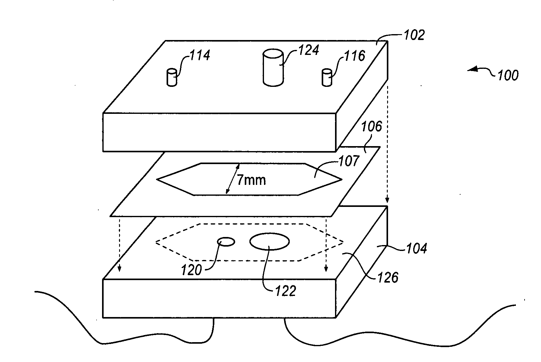
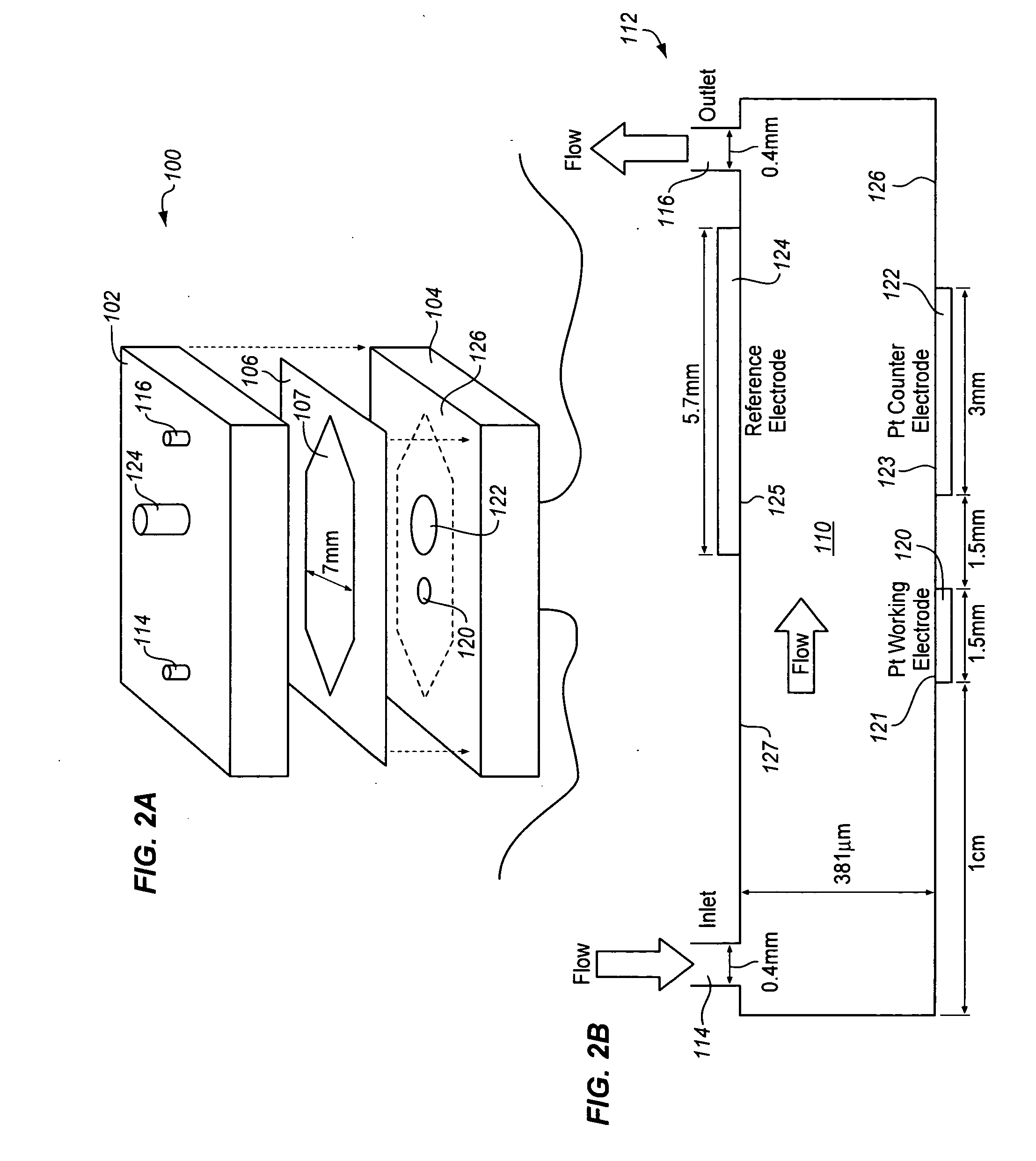
[0061]FIGS. 2A and 2B depict an exemplary flow-through cell 100 in accordance with the invention. FIG. 2A depicts schematically an expanded perspective view of flow-through cell 100 having top plate 102 and bottom plate 104. Plates 102, 104 are typically made from plastic or other electrically non-conductive material. Flow-through cell 100 also includes electrically non-conductive gasket 106 located between top plate 102 and bottom plate 104. When flow-through cell 100 is assembled (not shown in FIG. 2A), cut-out area 107 in gasket 106, together with top plate 102 and bottom plate 104, serves to define a flow channel 110, depicted schematically in cross-sectional view 112 in FIG. 2B. As depicted FIGS. 2A and 2B, a flow-through cell 100 further includes channel inlet port 114, channel outlet port 116, working electrode 120 having top surface 121, counter electrode 122 having top surface 123, and reference electrode 124 having bottom surface 125. In the exemplary embodiment, channel i...
example 2
[0068]An exemplary series of measurements in accordance with the invention were conducted at different known concentrations of organic accelerator additive in an electrolytic plating solution.
[0069]An electrolytic virgin make-up solution (VMS) contained in de-ionized water: 40 grams per liter (g / l) of dissolved copper metal, added as copper sulfate pentahydrate (CuSO4·5H2O); 10 g / l H2SO4; and 50 milligram per liter (mg / l) chloride ion, added as HCl.
[0070]The preconditioning solution consisted essentially of 15 milliliter (mL) of Enthone VIAFORM® EXTREME™ suppressor per liter of VMS. The functional species of VIAFORM® EXTREME™ suppressor consists essentially of a formulation having an average molecular weight of about 2500 and a molar ratio of polypropylene glycol (PPG) to polyethylene glycol (PEG) of about 0.5. A concentration of 15 milliliters per liter (mL / L) of VIAFORM® EXTREME™ suppressor in a plating solution corresponds to a concentration of about 1500 parts per million (ppm) ...
example 3
[0080]Indirect measurements of accelerator concentration were performed in accordance with the invention at various representative concentrations of suppressor and leveler at different nominal concentrations of accelerator. A representative exemplary electroplating bath solution has a composition of 9 mL / L Enthone VIAFORM® EXTREME™ accelerator, 2 mL / L Enthone VIAFORM® EXTREME™ suppressor, and 3 mL / L Enthone VIAFORM® EXTREME™ leveler in VMS; that is, a 9 / 2 / 3 solution using the notation of this specification. Representative requirements of a measuring system in a commercial electroplating system using a 9 / 2 / 3 playing solution include the ability to monitor organic plating additives within 5% accuracy within the following concentration ranges: accelerator, 9 mL / L±2 mL / L; suppressor, 2 mL / L±1 mL / L; leveler, 3 mL / L±1 mL / L. Accordingly, measurements were made using electroplating solutions having an accelerator concentration of 5 mL / L, 9 mL / L and 13 mL / L. At each of these three accelerato...
PUM
 Abstract
Description
Claims
Application Information