
Polymer for lithographic purposes and method for producing same

a technology of lithographic and polymer, applied in the direction of optics, basic electric elements, electric devices, etc., can solve the problems of insufficient cross-linking reaction efficiency of repulsing compound (polymer), low capacity of manufactured semiconductor devices, and low molecular weight of compound (polymer), so as to achieve high-precision operation and fine and sharp patterning

Inactive Publication Date: 2011-03-17
DAICEL CHEM IND LTD
View PDF4 Cites 0 Cited by
  • Summary
  • Abstract
  • Description
  • Claims
  • Application Information

AI Technical Summary

Benefits of technology

[0009]To solve the above problems, an attempt has been made to use a polymer containing hydroxyl groups and carboxyl groups in coexistence as reaction points with a divinyl ether, but it has been found that the polymer shows significantly lower etching resistance because of a larger content of oxygen atoms in the polymer, although the polymer is effective to reduce LER. Accordingly, an object of the present invention is to provide a polymer for lithographic purposes (resin for photoresists) and a production method thereof, a composition for lithographic purposes, and a method for manufacturing a semiconductor device using the composition for lithographic purposes, each of which can solve the above problems and allows very fine and uniform patterning in the manufacture of semiconductor devices.Solution to Problem
[0021]The polymers for lithographic purposes according to the present invention are cross-linked through acetal bonds each having an aromatic ring, and, when used for lithographic purposes, allow very fine and sharp patterning. They are therefore much advantageously usable in the manufacture typically of semiconductor devices even with high degree of integration, where highly accurate operations are especially required.

Problems solved by technology

Initially, i-line (i-ray) and g-line (g-ray) were used in lithographic exposure and gave patterns with broad line widths, and the manufactured semiconductor devices thereby had low capacities.
The technique of designing the polymer to have a lower molecular weight is effective from the viewpoint of reducing LER, but such a polymer having a lower molecular weight suffers from problems such that it develops crystallinity to have insufficient film-forming properties or has a lowered strength to cause pattern collapse.
This compound (polymer) is insufficiently efficiently cleaved into units of low molecular weights, because the compound has only one point (acetal structure), which is cleavable by the action of an acid, per its cross-linking chain.
The repulsing compound (polymer) shows a poor efficiency in cross-linking reaction, probably because the polymer uses, as cross-linking points through the divinyl ether, hydroxyl groups bound to a multivalent alicyclic hydrocarbon, and this causes steric hindrance.
In addition, the polymer does not effectively improve LER, because the polymer uses hydroxyl groups as reaction points with the divinyl ether and thereby does not significantly change in solubility in an alkaline developer between before and after cleavage of cross-links.
To have a sufficiently reduced molecular weight in polymer chains after exposure, this compound (polymer) should contain a large amount of carboxyl groups acting as cross-linking points and thereby shows an excessively high sensitivity with respect to an acid.
This reduces the maximum allowable limit in variation of the amount of generated acid, which variation is caused typically by fluctuations in exposure, and the polymer has poor handleability.

Method used


Image

  • Polymer for lithographic purposes and method for producing same
  • Polymer for lithographic purposes and method for producing same
  • Polymer for lithographic purposes and method for producing same

Examples


referential example 1

Synthesis of 2,6-Naphthalenediol Divinyl Ether

[0104]To a solution of a mixture of di-μ-chlorobis(1,5-cyclooctadiene)diiridium(I) [Ir(cod)Cl]2 (2.1 g, 3.1 mmol) and sodium carbonate (26.2 g, 312.2 mmol) in toluene (250 g) were added 2,6-dihydroxynaphthalene (25 g, 156.1 mmol) and vinyl propionate (62.5 g, 624.3 mmol), followed by stirring in an argon atmosphere at 110° C. for 4 hours. The reaction mixture was analyzed by gas chromatography to find that 2,6-bis(vinyloxy)naphthalene was formed in a yield of 55%.

[Spectral Data of 2,6-bis(vinyloxy)naphthalene]

[0105]1H-NMR (CDCl3) δ: 4.50 (2H, d), 4.81 (2H, d), 6.75 (2H, dd), 7.22 (2H, d), 7.30 (2H, s), 7.71 (2H, d)

referential example 2

Synthesis of 2,6-Naphthalenedimethylol Divinyl Ether

[0106]To a solution of a mixture of di-μ-chlorobis(1,5-cyclooctadiene)diiridium(I) [Ir (cod)Cl]2 (0.86 g, 1.3 mmol) and sodium carbonate (10.7 g, 127.5 mmol) in toluene (100 g) were added 2,6-naphthalenedimethanol (12.0 g, 63.8 mmol) and vinyl propionate (25.5 g, 255.0 mmol), followed by stirring in an argon atmosphere at 110° C. for 6 hours. The reaction mixture was analyzed by gas chromatography to find that 2,6-bis(vinyloxymethyl)naphthalene was formed in a yield of 40%.

[Spectral Data of 2,6-bis(vinyloxymethyl)naphthalene]

[0107]1H-NMR (CDCl3) δ: 4.11 (2H, d), 4.36 (2H, d), 4.92 (4H, s), 6.61 (2H, dd), 7.47 (2H, d), 7.81 (2H, s), 7.84 (2H, d)

synthetic example 1

Synthesis of Polymeric Compound of Following Structure

[0108]

[0109]In a nitrogen atmosphere, 128.9 g of propylene glycol monomethyl ether acetate (PGMEA) and 55.3 g of propylene glycol monomethyl ether (PGME) were placed in a round-bottom flask equipped with a reflux condenser, a stirring bar, a three-way stopcock, and a thermometer; and, while keeping the temperature to 90° C. and stirring, a solution mixture was added dropwise thereto over 5 hours, followed by further stirring at the same temperature (90° C.) for 2 hours. The solution mixture contained 26.5 g (127.3 mmol) of 5-acryloyloxy-3-oxatricyclo[4.2.1.04,8]nonan-2-one, 6.0 g (25.4 mmol) of 1-hydroxy-5-methacryloyloxyadamantane, 13.3 g (50.7 mmol) of 1-(1-methacryloyloxy-1-methylethyl)adamantane, 4.4 g (51.1 mmol) of methacrylic acid, 4.02 g of dimethyl 2,2′-azobis(isobutyrate)dimethyl (supplied by Wako Pure Chemical Industries Ltd. under the trade name “V-601”), 69.4 g of PGMEA, and 29.8 g of PGME. After being cooled, the po...


PUM

PropertyMeasurementUnit
Wavelengthaaaaaaaaaa
Molalityaaaaaaaaaa
Surface roughnessaaaaaaaaaa

Abstract

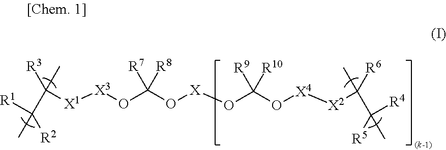
A polymer for lithographic purposes has at least a repeating structural unit represented by following General Formula (I). In Formula (I), R1, R3, R4, and R6 each independently represent hydrogen atom, a halogen atom, cyano group, an alkyl group, or a haloalkyl group; R2 and R5 each independently represent hydrogen atom, cyano group, etc.; X1 and X2 each independently represent single bond, or a substituted or unsubstituted bivalent alkylene, alkenylene, or cycloalkylene group, etc.; X3 and X4 each independently represent single bond or —CO—; R7, R8, R9, and R10 each independently represent hydrogen atom, an alkyl group, or a cycloalkyl group. The polymer for lithographic purposes shows good balance between line edge roughness (LER) and etching resistance and allows very fine and uniform patterning.

Description

TECHNICAL FIELD[0001]The present invention relates to a polymer for lithographic purposes (resin for photoresists) and a production method thereof, which polymer is used typically in fine patterning (microlithography) of semiconductor devices. The present invention also relates to a composition for lithographic purposes, and a method for manufacturing a semiconductor device using the composition for lithographic purposes.BACKGROUND ART[0002]Recent dramatic innovation on lithographic patterning techniques in the manufacture of semiconductors (semiconductor devices) has made design rules as line widths finer and finer. Initially, i-line (i-ray) and g-line (g-ray) were used in lithographic exposure and gave patterns with broad line widths, and the manufactured semiconductor devices thereby had low capacities. However, recent technological development has allowed the use of KrF excimer laser and further recently has allowed the use of ArF excimer laser to give patterns in accordance wit...

Claims


Application Information

Patent Timeline
IPC IPC(8): G03F7/004G03F7/20C08G63/08
CPCC08F216/125C08F220/06G03F7/0397C08F220/28C08F220/18C08F220/283C08F220/1818
Inventor OKUMURA, ARIMICHIINOUE, KEIZOOKAMOTO, KAZUKI
Owner DAICEL CHEM IND LTD
Learn More